

International Journal of Scientific & Engineering Research Vol ume 3, Issue 9, September-2012 1
ISSN 2229-5518
Abstract: A wide band bipolar amplifier is a signal amplifier that has the ability to emit more than one output signal . The output is determined by either the positive or negative polarity of the signal upon input to the amplifier circuit. The bipolar amplifier is not only able to emit multiple signals that correspond to the input polarity, but it is also able to add gain to the signal as the input signal is passed through it. This allows for an input signal that results in low noise incurrence, which is a common problem among different amplifier circuits.
The circuit layout of a bipolar amplifier is designed to minimize the amount of noise within the amplifier circuit itself. In fact, any amplifier used, whether bipolar in nature or not, must be designed in a manner that produces as little noise as possible. If the circuit is n ot designed to minimize
noise, the noise created will accompany the output signal in the form of an amplified signal.
The design of a bipolar amplifier is a simple one. The input signal is matched in noise impedance upon the receiving of the s ignal. Noise generated throughout a circuit is usually cau sed by the components located in the front end of the circuit itself, and the design of the bipolar amplifier minimizes this.
Bipolar amplifiers have an advantage over other amplifier circuits in the noise reduction aspect of the circuit due to the wa y the amplifier’s circuit
itself is laid out. Most of the noise that occurs within a circuit is caused by the continuous transfer of the input signal f rom circuit component to circuit component. The fact that the layout of a bipolar amplifier is not conducive t o the production of electronic noise and that the amplifier is usually located in the front end of the device circuit is a significant advantage to the amplifier.
Another advantage to using the bipolar amplifier at the beginning of a device circuit is tha t any noise in the input signal to the amplifier is
reduced through the natural noise-reducing tendencies of the amplifier. This is true regardless of the polarity of the input signal. As a result, bipolar amplifiers are often used in both AM and FM radio transmissions as a means of adding gain to the input signal’s power without adding gain to any noise in the signal itself.
Keyword: Wide band, Bipolar Amplifier,
—————————— ——————————
A bipolar amplifier is a signal amplifier that has the ability to emit more than one output signal. The output is determined by either the positive or negative polarity of the signal upon input to the amplifier circuit. The bipolar amplifier is not only able to emit multiple signals that correspond to the input polarity, but it is also able to add gain to the signal as the input signal is passed through it. This allows for an input signal that results in low noise incurrence, which is a common problem among different amplifier circuits.
The circuit layout of a bipolar amplifier is designed to minimize
the amount of noise within the amplifier circuit itself. In fact, any amplifier used, whether bipolar in nature or not, must be designed in a manner that produces as little noise as possible. If the circuit is not designed to minimize noise, the noise created will accompany the output signal in the form of an amplified signal.
The design of a bipolar amplifier is a simple one. The input
signal is matched in noise impedance upon the receiving of the signal. Noise generated throughout a circuit is usually caused by the components located in the front end of the circuit itself, and the design of the bipolar amplifier minimizes this.
Bipolar amplifiers have an advantage over other amplifier circuits in the noise reduction aspect of the circuit due to the way the amplifier’s circuit itself is laid out. Most of the noise that occurs within a circuit is caused by the continuous transfer of the input signal from circuit component to circuit component. The fact that the layout of a bipolar amplifier is not conducive to the production of electronic noise and that the amplifier is usually located in the front end of the device circuit is a significant advantage to the amplifier.![]()
Another advantage to using the bipolar amplifier at the beginning of a device circuit is that any noise in the input signal to
1Student of Master Technology in Electronic Communication, Jan Nayak Choudhary
Devi Lal Memorial College of Engineering, Sirsa
2Assistant Professor In ECE Department, Jan Nayak Choudhary Devi Lal Memorial
College of Engineering, Sirsa,
the amplifier is reduced through the natural noise-reducing tendencies of the amplifier. This is true regardless of the polarity of the input signal. As a result, bipolar amplifiers are often used in both AM and FM radio transmissions as a means of adding gain to the input signal’s power without adding gain to any noise in the signal itself
Before digging into actual op-amp specifications, it is worthwhile to take a brief look at each of these process technologies. Bipolar transistors, invented in the late 1940s at Bell Laboratories, are so named because they use both electrons and holes in their operation. These transistors were used extensively in the design of ICs for decades, and are still in use today.
Complementary metal-oxide semiconductors (CMOS) came in
the 1960s and became popular as lower-power digital-logic alternatives to transistor-transistor logic (TTL). Unlike other transistor types, CMOS transistors only draw current when switching states — hence, their association with low power.
As the name implies, BiCMOS combines both bipolar and CMOS technologies on the same device. This combination allows the IC designer to take advantage of the inherent benefits of each technology. Until the last couple of decades, combining bipolar and CMOS into one seamless process was not very reliable, and was very costly. Today, BiCMOS is used for certain applications (including op amps) where the inherent benefits outweigh the additional costs associated with this process.
In the end, each of these process technologies has advantages
and disadvantages when it comes to op-amp design. The following sections will take a closer look at these tradeoffs and how they relate to actual amplifier specifications.
© 2012 w.ijser.org

International Journal of Scientific & Engineering Research Vol ume 3, Issue 9, September-2012 2
ISSN 2229-5518
![]()
As mentioned above, CMOS is known for lower power, as the transistors only draw current when switching states. However, this power advantage is only true for slower amplifiers.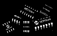
Fig.1. CMOS op amps, like the MCP6041 from Microchip Technology, provide low quiescent current for low-power applications.
![]()
As bandwidth increases, a CMOS amplifier’s current increases dramatically, and soon draws more current than a comparable bipolar amplifier. Because of the exponentially increasing current required for CMOS to achieve high speeds, bipolars are typically better suited for high-bandwidth, high-slewing applications.
For lower-bandwidth applications, CMOS amplifiers can still
provide power advantages. For example, the MCP6041 low-power CMOS op amp from Microchip Technology has a typical quiescent current of only 600 nA and provides a gain-bandwidth-product of 14 kHz.
In terms of flicker or 1/f noise, CMOS transistors have worse low-frequency noise than bipolar transistors. At low frequencies, this noise is dominated by irregularities in the conduction path and noise due to the bias currents within the transistors. In a bipolar transistor, the conduction path is buried down inside the silicon.
On a CMOS transistor, the current flow is near the surface, making it susceptible to defects in the surface of the silicon, which increases the low-frequency noise. At higher frequencies, 1/f noise is negligible as the white noise from other sources begins to dominate.
CMOS transistors have a lower transconductance, relative to similarly sized bipolar transistors, which results in higher broadband noise. In general, bipolar op amps hold an inherent advantage over CMOS when it comes to noise performance.
Another important amplifier specification is input offset voltage. As the name implies, this specification is the amplifier’s voltage difference between the inverting and non-inverting inputs. This error voltage can vary from microvolts up to millivolts, and is highly dependent on how well matched the input transistors are.
Bipolar transistors inherently offer better matching, resulting in
lower offset voltages for a given architecture. Some manufacturers compensate for this inherent mismatch by using laser trimming, fuses, or even EPROM.
These techniques can improve an amplifier’s performance
significantly, regardless of the process technology. Better matching also results in less voltage-offset drift over temperature, which is also an important consideration in many applications. .
All amplifiers have a specification called input bias current, the amount of current flow into the inputs of an amplifier to bias the input transistors. This current can be thought of as leakage current, but is referred to as bias current when on the inputs of an amplifier. This bias current can range from picoamperes to hundreds of nanoamperes.
Op amps with a CMOS input stage generally have less bias current than those with bipolar input transistors, typically around 1 pA, while bipolar transistors can be orders of magnitude higher. This bias current is converted into a voltage through the circuitry’s input resistance, and ends up resulting in an error voltage at the output of the amplifier. The less bias current the better, and in this regard CMOS has a distinct advantage. .
A wideband amplifier circuit provides high current gain and a wide bandwidth by employing only npn transistors, which have better high-frequency characteristics than those of pnp transistors, in the signal path. Wideband current amplification is achieved using npn transistors in a current-mirror configuration, with base-emitter voltage matching to permit the current gain to be easily set as a function of transistor area. The wideband amplifier circuit can also be used in a differential wideband amplifier configuration to obtain a combination of high current gain, wide bandwidth and wide output swing not obtainable with conventional differential amplifiers.![]()
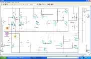
Fig. 2 Wide band amplifier circuit Using NPN transistor Stages of wide band bipolar amplifier:-
Here we define the stages of wideband bipolar amplifier.
Class A operation (like the common-emitter/common-collector transistor circuits) is defined by having a bias level that maintains an output current at all times, irrespective of the input signal level. This is typical of small signal amplifiers and result in a low distortion output. Amplifier circuits designed to deliver large output currents capable of driving low impedance loads result in transistor heating and without proper heat sinking thermal run away can cause destruction of the amplifier circuit. Because of the need for large output current it becomes impractical and inefficient to run the transistors such that they only operate over a very small proportion of their available range. This is the how all small signal amplifiers produce approximately linear characteristics.
Formatted: Centered
IJSER © 2012 http://www.ijser.org

International Journal of Scientific & Engineering Research Vol ume 3, Issue 9, September-2012 3
ISSN 2229-5518
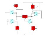
stage is used to receive the output current which is generated by the transistor NPN and NPN2. In other word we can say that the output of transistor NPN and NPN2 are the input of the post-amplifier stage.
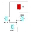
Fig. 3 Push pull amplifier
If some percentage of an amplifier’s output signal is connected
to the input, so that the amplifier part of its own output signal, we have what is know as feedback. Feedback comes in two varieties:
Fig.6 Post amplifier

positive (also called regenerative), and negative (also called degenerative). Positive feedback reinforces the direction of an amplifier’s output voltage change, while negative feedback does just the opposite. Here the feedback is used for give the feedback signal to the push pull amplifier. In feedback amplifier stage NPN transistor, capacitor and resistance with the help of these we can give the signal to the push pull amplifier.
Fig.4 Feedback amplifier
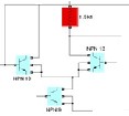
A preamplifier (preamp) is an electronic amplifier that prepares a small electrical signal for further amplification or processing. A preamplifier is often placed after the push pull amplifier to reduce the effects of noise and interference. It is used to boost the signal strength to drive the cable to the main instrument without significantly degrading the signal-to-noise ratio (SNR). The noise performance of a preamplifier is critical according to Friis's formula, when the gain of the preamplifier is high, the SNR of the final signal is determined by the SNR of the input signal and the noise figure of the preamplifier. The pre-amplifier stage is used to receive the output current which is generated by the transistor NPN1 and NPN3. In other word we can say that the output of transistor NPN1 and NPN3 are the input of the pre-amplifier stage.
A HIGHLY linear npn-only bipolar wide-band intermediate-
frequency (IF) amplifier is built using a topology previously reported for a complementary metal–oxide– semiconductor (CMOS) amplifier [1]. The main motivation for building amplifiers in both bipolar and CMOS is that we want to be flexible in the choice of technology. In a system with several building blocks on the same chip, the requirements of the other parts may then determine which technology to use.
Since the inter modulation noise is critical for the performance of a
wide-band IF amplifier, the nonlinearity must be minimized. To achieve this, we use the same techniques as in [1]. A push–pull class A output stage is used together with a double-nested Miller compensation to maximize the feedback around it [2], [3]. To cancel out even-order distortion, the topology is fully differential.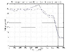
Fig.6
Fig.5 Pre-amplifier
The post amplifier is used to increase the electrical signal to the level required for future signal processing. Here the post amplifier
IJSER © 2012 http://www.ijser.org

International Journal of Scientific & Engineering Research Vol ume 3, Issue 9, September-2012 4
ISSN 2229-5518
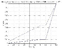
amplifier. We use a resistor loaded differential stage with differential output as input stage. The desired voltage gain of the entire amplifier is 100, and the maximum output amplitude is about 6, resulting in about 60 m maximum input signal amplitude. If the input stage is not to degrade the linearity, emitter degeneration must then be employed. The drawback is a degraded noise performance.
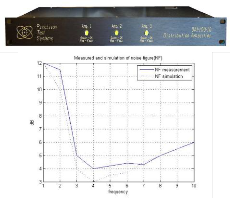
Fig.7
As in the CMOS amplifier, we use a push–pull class A output stage for best linearity. To accomplish push–pull operation, an emitter follower arrangement is used (see Fig. 6).
This reduces the output voltage swing, and a 5-V supply is therefore used.
The output transistors are and , where is connected as a follower. As the stage is biased in class A, the transistors are on all the time. The output voltage therefore essentially follows the base voltage of. When the collector current of is low, the output voltage is therefore high. The collector current of is then also low, as it is connected in parallel with. Fig.6. The output stage. Fig.7. The input stage. is high, the output is low and the current of is high. The stage is thus a push–pull stage. If the quiescent collector current of transistor is high enough, the stage will operate in class A. The collector current through is the same as through scaled by their emitter areas. The quiescent collector current of is determined by and the quiescent output voltage, that is fixed by a common mode feedback circuit. The bias of the output stage is thus determined by and the emitter area ratio of and.
Unlike most competitive units, the DA1-100-10 accepts inputs from +7 dBm to +20 dBm (-20 dBm to +30 dBm optional) and provides outputs from 0 dBm to > +13 dBm (up to +20 dBm optional). The output will not vary with input variations.
This is very useful when long cable runs are being used or
equipment have different input level requirements. The AGC can be disabled, if required, making the unit a fixed gain amplifier. Different gains are available upon request.
There are five, ten or fifteen sine wave outputs with a bandwidth from 1 to 100 MHz (usable to 150 MHz). Each output is completely isolated from the input and each other. Therefore the reference oscillator connected to the DA1-100-10’s input is protected against load variations, short circuits etc. that may be applied to the outputs.
Channel to channel isolation is > 90 dB at 10 MHz and > 65 dB
at 100 MHz. Output to input isolation is > 130 dB at 10 MHz and >
100 dB at 100 MHz. Each output port can be independently set to any level from 0 to > +13 dBm on the standard unit and outputs to
+20 dBm are optional available. The ability to set every output to a
different level is very useful when dealing with equipment that has different input level ranges. Over 1000 outputs can be obtained without any significant increase in close-in noise.
To provide more gain, a long tailed pair (LTP) stage (,) precedes the push–pull stage. This stage also provides some level shift, which is needed as no PNP devices are allowed. The absence of PNP devices also makes it necessary to use a resistor.
As trans resistance output stages are used, the input stage must be a trans conductance if the cascade is to become a voltage
IJSER © 2012 http://www.ijser.org

International Journal of Scientific & Engineering Research Vol ume 3, Issue 9, September-2012 5
ISSN 2229-5518
The DA1-100-10 has very low phase noise. This enables units to be connected in series without adding any appreciable noise to the reference input. With only three DA1-100-10’s in series, up to 1000 outputs can be derived from one input.
A typical plot of phase noise is shown below. The blue line is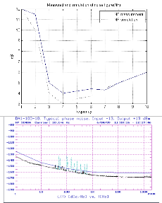
the DA1-100-10’s specifications. The light blue lines are line related, spurious outputs. These spurs (50 or 60 Hz) are present in any equipment connected to the AC 115 or 230 VAC supply. The black line is the actual phase noise. The far out noise (offsets > 1 kHz) can even be improved upon by careful selection of the output level and amplifier gain. Floor noise to 171 dBc/Hz is achievable.
The wide frequency bandwidth allows the outputs to have stable phase. The phase stability is typically 5 ps/°C. Also the delay match between outputs is better than 2.2 ns overall and typically less than
350 ps between groups of five outputs.
Every output has alarm monitoring. Should the RF level drop on
any output, an alarm will be raised. Also front panel LED’s shows
the status of the alarms. The alarm signals are also available on the rear panel.
The DA1-100-10 Distribution Amplifier is ideal for use in calibration or standard laboratories, space research, satellite systems, communication systems or anywhere where ultimate performance is needed.
![]()
Precision Test Systems also manufacturers the PTS50 and DA1010 series of distribution amplifiers. These models are lower cost alternatives to the DA1-100-10 but still give very good performance.
This topology can be used for npn-only bipolar wide-band IF amplifiers, as well as CMOS. A bipolar circuit with the same power consumption as one in CMOS was made. The bipolar amplifier has higher linearity, since the bipolar devices are faster and have higher trans conductance than CMOS for similar operating conditions.
Drawbacks of the bipolar circuit, caused by the absence of pnp devices, are smaller common-mode input voltage range and a higher supply voltage. In a BiCMOS circuit, P-channel MOS devices can be used instead of pnp. By using a current mirror load in the LTP stage, the loop gain could then be doubled. Without reducing the performance, the power consumption could be reduced because of the reduced supply voltage and the current mirror.
1. A.S. Sedra and K.C. Smith (2004). Microelectronic Circuits
(5th ed.). New York: Oxford University Press. p. 397, Figure
5.17, and p. 1245. ISBN 0-19-514251-9
2. Alphonse J. Sistino (1996).Essentials of electronic circuitry.
CRC Press. pp. 64. ISBN 9780824796938
3. Written By: Alexis W. Edited By: Heather Bailey. Copyright
Protected: 2003 2011 Conjecture Corporation
4. Eglin, J. M. A Direct Current Amplifier for Measuring Small Currents. Journal of the Optical Society of America and Review of Scientific Instruments, May 1929, p.393-402.
5. Matthews, B. H. C. A Special Purpose Amplifier. The Journal of
Physiology, March 17 1934, 81, 28P-29P.
6. Blumlein, A. D. UK Patent No: 482740; July 4, 1936. US Patent
2185367; filed June 24, 1937
IJSER © 2012 http://www.ijser.org

International Journal of Scientific & Engineering Research Vol ume 3, Issue 9, September-2012 6
ISSN 2229-5518
7. Offner, F. Push-Pull Resistance Coupled Amplifiers. Review of
Scientific Instruments, January 1937, p.20-21.
8. Schmitt, O. H. Cathode Phase Inversion. Review of Scientific
Instruments, 1937, p.100-101.
9. Geddes, L. A. Who Invented the Differential Amplifier?. IEEE Engineering in Medicine and Biology, May/June 1996, p.116-
117.
IJSER © 2012 http://www.ijser.org