International Journal of Scientific & Engineering Research, Volume 6, Issue 2, February-2015 791
ISSN 2229-5518
Universal Sensor Interface Circuits Performance
Evaluation for Multi Sensor Systems
Siti Nur Syuhadah Baharudin, Asral Bahari Jambek and Rizalafande Che Ismail
School of Microelectronic Engineering, University Malaysia Perlis
n modern technologies, smart sensor systems will be im- portant in future applications such as in the fields of bio- medicine, industry and agriculture. For example, in the bio- medical field, sensor systems are used to detect temperature, glucose and blood pressure without the use of wires. This can reduce the installation costs and allow the devices to be easily positioned at any desired points. There are many challenges when designing sensor systems such as interfacing the circuit with various types of sensors and minimizing the power con- sumption. Typical sensor interface circuits can only support one specific application at a time. However, current applica- tions require a combination of different sensors in single de- vices [2]. Therefore, a sensor interface circuit that can receive input from various sensors is needed [2]. To solve this prob- lem, multi sensor interfaces or universal sensor interfaces have been introduced. This circuit can reduce the design cost where it can intelligently read and process different sensor applica-
tion [3].
This paper highlights several architectures for multi sensor interface circuits that have been proposed in the literature. The architectures will be discussed and compared to identify the best sensor interface architecture implementation. This paper is organized as follows. Section 2 discusses the existing meth- ods used to implement universal sensor interface circuits. Sec- tion 3 discusses their performance comparison in terms of speed, area and power. Finally, Section 4 concludes the paper.
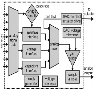
The author in [3] proposed the circuit as shown in Figure
1.The circuit consists of six main modules. They are the ana-
logue signal router, the interface circuit, the analogue multi-
plexer, the digital to analogue converters (DACs), the pro-
grammable gain-stage, and a sample and hold stage. The ar-
chitecture uses an analogue signal router to interface with var- ious sensors. This router allows various sensor inputs to be connected before separating them into either a voltage, capaci-
tive or resistive sensor. Then, the signal goes to the program- mable gain stage, followed by a sample and hold stage before passing to the output.
Paper [4] utilizes analogue multiplexer and bridge circuits to reduce the overall cost as shown in Figure 2. The analogue multiplexer receives various signal inputs and channels the output to either the capacitive or resistive bridge. The output from the bridge will be passed to a shared pre-amplifier and signal conditioning circuit. The conditioned signal will be converted to a digital signal by the sample and hold, and ana- logue to the digital converter (ADC) circuit. Based on the ar- chitecture on Figure 3 [5], the authors focused on making their design simple by combining the resistive and capacitive inputs with the use of a capacitive sensor that uses a resistive refer- ence and vice versa.
The authors implemented the exclusive OR (XOR) logic gate to produce digital pulse with a duty cycle proportional to the sensed capacitance or resistance without using any ADC. Next, the digital signal is fed into a decimator. Based on the architecture on Figure 4 [6], the design consists of an interface circuit, an ADC, a local configuration module and timing cir- cuits. The circuit operates when the sensor element senses one or more physical quantities such as temperature, motion, or gasses. The interface circuit consists of an analogue multiplex- er, a programmable gain and a sample and hold stage and outputs the result to the ADC. The measured data is then stored before transmitting it wirelessly to the receiver. Com- pared to previous circuits, this design only accepts input from capacitive sensors.
Figure 5 shows the architecture as discussed in [7]. The circuit consists of a multiplexer, reconfigurable signal conditioning, a voltage-to-frequency converter, and a microcontroller. The sensors’ inputs are connected directly to the multiplexer be- fore output he signal to the reconfigurable signal conditioning. From here, the signal is then converted using a voltage-to- frequency converter (VFC). The VFC removes the need to use an ADC to digitize the conditioned signal. As discussed in [7],
IJSER © 2015 http://www.ijser.org
International Journal of Scientific & Engineering Research, Volume 6, Issue 2, February-2015 792
ISSN 2229-5518

Fig. 1. Architecture [3]

Fig. 2. Architecture [4]
The VFC has better noise immunity, wide dynamic range, and good accuracy. The output from the VFC is then fed into the microcontroller. This design has the advantage of lower cost but with the disadvantage of a slower conversion time [10].
Based on the existing literature, we can conclude that for uni- versal sensor interfaces, there are three main modules to be considered. These modules are signal selection units, signal condition units and signal conversion units.
In most architectures discussed in Section 2, the signal selec-
tion unit is performed using a multiplexer. Papers [3], [4], [6] and [7] utilize a multiplexer to select the signal. In paper [5], the signal selection is unique in that it uses sensing capaci- tance or resistance to produce a digital signal where the duty cycle output is proportional to the sensing capacitance or re- sistance value.
Fig. 3. Architecture [5]
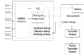
Fig. 4. Architecture [6]
IJSER © 2015 http://www.ijser.org
International Journal of Scientific & Engineering Research, Volume 6, Issue 2, February-2015 793
ISSN 2229-5518
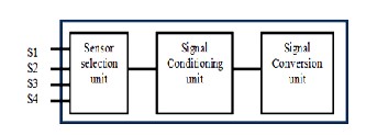
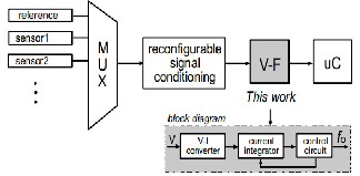 Fig. 6. Typical Universal Sensor Interface Circuit Module
Fig. 5. Architecture [7]
inputs. Compare to architecture [4], [5] and [7], that use of
0.18µm CMOS, architectures [5] and [7] shows the smallest area. However, in terms of power consumption, the architec- ture in [7] dissipates the largest power consumption compared to the other architectures.
Once the signal has been selected from various sensor inputs, it will be passed to the signal conditional module. The pur- pose of this interface is to convert low level sensor outputs to useful electronic signals. Compared to other circuit architec- tures, the design in [7] implements a reconfigurable signal conditioning to take into account the variety of the input types.
The signal conversion module plays an important role in universal sensor interface circuits since it provides useful in- put to any digital signal processing module. From the dis- cussed papers, various methods are used to convert the signal such as using ADCs. However, paper [5] and [7] perform a different type of conversion. In [5], instead of using an ADC, the circuit converts the analogue signal to a digital pulse that has a duty cycle proportional to the input voltage signal. In [7], the author utilizes voltage-to-frequency signal conversion before it is read by the microcontroller using the internal timer as shown in Figure 5.
While signal conversion can be performed using different methods, each method has different advantages and disad- vantages. Table 1 compares the advantages and disadvantages of this circuit. From Table 1, the usage of the voltage-to- frequency conversation circuit as the signal conversation cir- cuit is attractive since this circuit is more versatile compared to other approaches. This circuit has low complexity and low design cost, and it can match the performance of many com- mercial A/D converters.
Table 2 compares the overall performance of the circuits in [3] to [7]. The table compares the size, power, input type, pro- cess technology and circuit features. Since each circuit is de- signed using different technology, comparing their perfor- mance is not a straight forward matter. Based on the table, architecture [3] provides a wider range of input sensors whereas architecture [6] only accepts input from capacitive
In this paper, the five existing universal sensor interface archi- tectures have been discussed and compared. Based on the comparison, a universal sensor interface requires three main modules. They are a signal selection unit, a signal condition- ing unit and a signal conversion unit. Since different signals perform differently, such as the signal condition module needs to be designed to accommodate different types of signal condtion module needs to be designed to accommodate dif- ferent types of signal characteristic, for the signal conversion module, an ADC, VFC and digital pulse width duty cycle can be used.
The authors would like to thank for Dr.Asral Bahari Jambek, Dr. Rizalafande Che Ismail, Technicians and PLV in the ad- vance ic design lab, Universiti Malaysia Perlis for helping, discussion, training and support on the circuit design.
[1] G. Chao, L. Xiujun, and G. C. M. Meijer, "A System-Level Approach
for The design of smart sensor interfaces," IEEE Sensors Conf., vol.1, pp. 210-21 October 2004..
[2] J. Zhang, A. Mason, “Characterization of a configurable sensor signal conditioning circuit for multi-sensor microsystems,”IEEE sensors conf.,vol.1, pp.198-201,October.2004.
[3] J. Zhang, J. Zhou and A. Mason, “Highly Adaptive Transducer Interface Circuit for Multi-Parameter Microsystems,” IEEETrans. Circ. Sys. I, vol. 54, no. 1, Jan. 2007.
[4] C. Yang, J. Xi, A. Mason, P. Zhong, "Configurable Hardware- Efficient Interface Circuit for Multi-Sensor Microsystems",IEEE Sensors 2006, Daegu, Korea, Oct.2006
IJSER © 2015 http://www.ijser.org
International Journal of Scientific & Engineering Research, Volume 6, Issue 2, February-2015 794
ISSN 2229-5518
[5] J.H.L.Lu, M. Inerowicz, S. Joo, J.K. Kwon, B.Jung,” A Low-Power,
Wide-Dynamic-Range Semi-Digital Universal Sensor Readout Circuit
Using Pulsewidth Modulation” IEEE sensors Journal, vol.11.n0 5 pp.
1132-1144, May 2011
[6] W. Bracke, P. Merken, R.Puers, C. Van Hoof,” Generic architectures and design methods for autonomoussensors”,sensor and actuators, 11 september 2006.
[7] B. Calvo, C. Azcona, N. Medrano, S.Celma,”A Low Cost VFC for
Low Power Sensor Interface”, Industrial Electronic(ISIE), 2010
IEEE International Symposium on,4-7 July 2010.
[8] J. Xi, C. Yang, A. Mason, P. Zhong, “Adaptive Multi-Sensor Interface
System-on-Chip”, IEEE Sensors Conference, Daegu, Korea, Oct. 2006 [9] B.Calro,N.Medrano, S. Celma and M.T sanz, “A Low –Power High
Sensitivity Cmos Volatge-to- Frequency Converter”, IEEE
international Symposium, pp.118-121, 2009.
[10] M.Strok, “New ![]() voltage to frequency converter”, IEEE, pp.631-
voltage to frequency converter”, IEEE, pp.631-
634,2002
[11] Floyd Mano,”Digital Electronics Design”, Prentice Hall,3th edition,
2002.
TABLE 1
COMPARISON PROS AND CONS REGARDING SIGNAL CONVERSATION
TABLE 2
COMPARISON OF UNIVERSAL SENSOR INTERFACE
(USI)
Pros | Cons | |
ADC | Low power, low hardware complexity and good robust- ness | Introduce extra noise |
Pulse | Low power | |
VFC | Low cost | Low conversation time |
IJSER © 2015 http://www.ijser.org