by consideration of Aspect ratio(W/L) of nMOS and pMOS. in
International Journal of Scientific & Engineering Research, Volume 5, Issue 8,August-2014 957
ISSN 2229-5518
subthreshold SRAM bit cell topologies for ultra low power applications
Mahipal Dargupally, T. Vasudeva Reddy
Padmasri Dr. B.V Raju Institute of Technology,Dept. of ECE,(CVD),Narsapur,Medak(Dt),India
Abstract— Ultra Low Power is one of the major concern in VLSI Industry recent years. One of the technique which used to improve the concept is Sub- threshold Logic Design. A Number of researchers considering this technique for developing ultra low power applications. The proposed paper is using Sub-threshold logic design for memory devices such as SRAM and observed the power consumption, leakage power and delay for different SRAM Bit Cells like 6T,8T,9T and 10T. It's used High Vth NMOS for reducing the power consumption and leakage power[1].
The comparative result between different SRAM Bit cells showing the percentage of reduction of power consumption and leakage power is
improved in 8T SRAM and delay in 9T SRAM than that of 6T SRAM. the different technology libraries like 90nm, 45nm have been used for thes e
SRAM bit cells design and analysis. CADENCE VIRTUOSO schematic editor is used for circuit design and analysis.
Index Terms— Low Leakage, Low Power, SRAM, Sub-Threshold, Weak inversion.
—————————— ——————————
HE Digital sub-threshold circuit design has become a very promising method for ultra-low power applications. Cir- cuits operating in the sub-threshold region utilize a sup-
ply voltage (VDD) that is close to or even less than the thresh- old voltages (Vth) of the transistors. This low VDD operation results in ultra low-power dissipation. The circuit operating from strong inversion, moderate inversion regions to weak inversion region can be known as sub-threshold operating region[2].
SRAMs comprise a significant percentage of the total
area and total power for many digital chips. SRAM leakage
can dominate total chip leakage. Lowering VDD for SRAM saves leakage power and access energy[3]. 6T-SRAM read and writes operations depend on static noise margin (SNM). Write operation is successful if bitcell becomes monostable and SNM value is negative. Read operation can be done if WL is ‘1’ & BL precharged to ‘1’.
Sub-threshold SRAM provides an advantage in min- imizing total memory energy consumption and providing compatibility with minimum-energy sub-threshold logic.
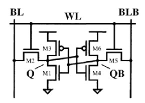
Fig.1 shows the standard 6T SRAM bitcell. it consist of two cross coupled inverters made up of M1,M3,M4,M6 and access transistors M2,M5[3]. the WORDLINE(WL) is connected to the gate terminal of an access transistors and BITLINE(BL) is connected to the drain terminal. WL is used to select the cell for accessing the transistor for operating the bit cell and BLs are used to perform the read and write operation.The written data is stored at the node 'Q' and its complement at the node
'QB'[3].
A. Write Mode
The proper write operation can be done successfully
by consideration of Aspect ratio(W/L) of nMOS and pMOS. in
Fig1 :standard SRAM6T Bitcell operation
sizing of transistors in SRAM bit cell nMOS should win the ratio fight with pMOS. if we want to write data'1' making the WL=1 and one of the bitline keeping High i.e BL=1 and BLB=0 then the value is been written as '1' at nodeQ and its comple- ment at nodeQB.
B. Read Mode
the read operation can be done by precharging the
Bitlines i.e BL=BLB=1 and now making the WL=1. then one of
the Bitline is making low value. the read value can be ob-
served by using Sense Amplifier.
This paper explores the design of SRAM cell with alternative Bitcells like 6T,8T,9T and 10T. the design of bitcells are used High Vth nMOS transistors for reducing the Leakage Pow- er[1]. the ratio's of nMOS and pMOS are maintained with de- sign considerations. the Drive transistors(M1,M4) should be stronger than that of Access transistors(M2,M5) to minimize the disturbance in the READ MODE. and in the WRITE MODE Access transistors should be strong than Load transis- tors(M3,M6) for successful write operation.
IJSER © 2014 http://www.ijser.org
International Journal of Scientific & Engineering Research, Volume 5, Issue 8,August-2014 958
ISSN 2229-5518
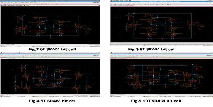
A. 8T Subthreshold SRAM Cell
The Fig.3 shows 8T SRAM bit cell is designed with two sleep
transistors connected as pull down transistors[5] to achieve the
low power design. to write '1' into SRAM cell the WL is assert-
ed and BL is made High and BLB is Low. to write '0' BL is low
and BLB keeping high. the values of '0'or'1' can be stored at
node Q and its complement at nodeQB. reading the stored
value at nodeQ by precharging operation. after precharging
the BitLines (BL=BLB=1) asserting the WL and pulling down
the one of the BitLine low.
B. 9T Subthreshold SRAM Cell
The Fig.4 shows proposed 9T SRAM bitcell is for sim-
ultaneously reducing leakage power and enhancing data sta-
bility. The upper sub-circuit of the memory cell is essentially
same 6T SRAM cell. The two write access transistors (M2,M5)
are controlled by a write signal (WL). The data is stored within
this upper memory sub-circuit. The lower sub-circuit of the
new cell is composed of the bitline access transistors (M7,M8)
and the read access transistor (M9). The operations of M7 and
M8 are controlled by the data stored in the cell. M9 is con-
trolled by a separate read signal(RD)[4].in write operation WL
is asserted and making High and Read signal RD is main-
tained low. now access transistors(M2,M5) are turned ON.
then the data can be stored at nodeQ. and this data can be
Read by asserting read signal RD to high and WL to low.
C.10T Subthreshold SRAM Cell
The Fig.5 shows 10T SRAM Bitcell is designed with
latch and two pass transistors. in design the high Vth nMOS
transistors are used to reduce the bitline leakage in read mode
and hold mode. the operation is used two word lines.
The separate WL and W_WL are used for accessing
the access transistors and drive transistors respectively. WL is
used for write operation and W_WL is used for controlling the storage node transistors. RWL is used for improve read operation[1].
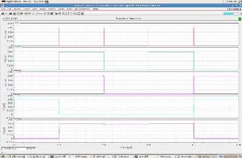
D. Performance Characteristics
The operation characteristics for READ and WRITE modes has
been shown for proposed 8T SRAM bit cell for supply voltages
VDD 0.8V(Fig.6) and 0.2V Fig.7 shows performance character-
istics of 8T SRAM Bit Cell for WRITE and Fig.8 is for READ
mode in subthreshold region.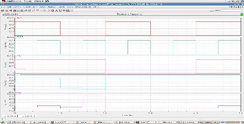
Fig.6 performance characteristics of 8T SRAM CELL for read and write mode for VDD 0.8V
This paper explores the different SRAM bit cell design, opera- tions and analysis of different parameters like power con- sumption, leakage power and delay in the sub threshold re- gion. the measurements have been observed over the range of voltages 0.8V down to the sub threshold region in 90NM and
45NMtechnologies.comparisions of all the bit cells for meas
IJSER © 2014 http://www.ijser.org
International Journal of Scientific & Engineering Research, Volume 5, Issue 8,August-2014 959
ISSN 2229-5518
2.62E-05
4.10E-07
6.40E-09
1.00E-10
6T
8T
9T
10T
Fig.7 performance characteristics of 8T SRAM CELL for write mode for VDD 0.2V
-urement parameters have been shown with respect to tech- nologies[7].
1.56E-05
6.25E-07
2.50E-08
1.00E-09
0.8 0.6 0.5 0.4 0.3 0.25 0.2
6T
8T
9T
10T
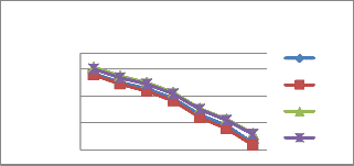
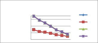
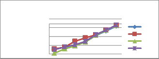
Fig.9 power consumption for write and read mode
1.56E-06
6.25E-08
2.50E-09
1.00E-10
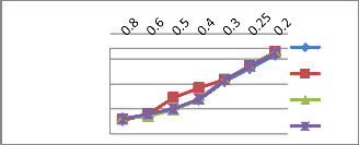
Fig.10 leakage power for various SRAM bit cells
6T
8T
9T
10T
Fig.8 performance characteristics of 8T SRAM CELL for read mode for VDD 0.2V
A. Performance characteristics of various SRAM BIT CELLS
in 90nm technology
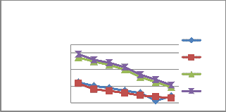
in 90nm technology the parameters like power consumption, leakage power and delay are shown below(Fig9-11)
power consumption and leakage power hasbeen reducing by by reducing the supply voltage VDD from 0.8 to 0.2v where delay is increasing.
B. Performance characteristics of various SRAM BIT CELLS in 45nm technology
In 45nm technology it performs same as 90nm technology. but it showing the variation in delay.
6.25E-09
1.25E-09
2.50E-10
5.00E-11
1.00E-11
6.25E-09
1.25E-09
2.50E-10
5.00E-11
1.00E-11
VDD(v)
6T
8T
9T
10T
6T
8T
9T
10T
power consumption and leakage power has been reducing by reducing the supply voltage VDD from 0.8 to 0.2v where delay is increasing.
Fig.11 delay for write and read mode
IJSER © 2014 http://www.ijser.org
International Journal of Scientific & Engineering Research, Volume 5, Issue 8,August-2014 960
ISSN 2229-5518
C. comparison of technological versions Vs parameters in sub- threshold region
• 90nm technology at supply voltage 0.2v:
Parameters | 6T | 8T | 9T | 10T |
power cosumption (nw) | 2.215 | 1.777 | 6.829 | 6.276 |
leakage power | 1.241nW | 453.9pW | 1.009nW | 1.13nW |
delay(nsec) | 1.93 | 1.973 | 1.841 | 1.971 |
• 45nmtechnology at supply voltage 0.25v:
Parameters | 6T | 8T | 9T | 10T | |
power con- sumtion(pw) | 113.8 | 103.9 | 165.2 | 145.9 | |
leakage pow- er(pw) | 26.11 | 17.02 | 19.01 | 26.02 | |
delay(psec) | 11.99 | 63.43 | 2.541 | 54.05 |
The authors would like to thank Dr.I.A.Pasha,HOD, ECE De- partment, BVRIT. This work was done in CVD(CENTER FOR VLSI DESIGN) Lab and expressing thank to coordinator Dr.I.B.K Raju and Asst.Prof Gnaneshwara Chary . They also express their sincere gratitude to the BVRIT, Narsapur, medak and thanks to parents, friends & colleagues for their contribu- tion in all aspects.
The paper has been shown that the comparative results of power consumption, leakage power and delay for both read and write modes of operations in various technologies such as
90nm and 45nm with various SRAM Bit cells. its observed that the leakage power and the power consumption is reduced in
8T SRAM Bit cell and delay is reduced in 9T SRAM Bit cell than 6TSRAM Bit cell. in subthreshold region its observed that the standard SRAM bit cell performance is given less priority than 8T and 9T SRAM bit cells. the leakage power is reduced by using the high Vth nMOS transistors.
[1] Wei-Bin Yang, Chi-Hsiung Wang, I-Ting Chuo, Huang-Hsuan Hsu" A
300 mV 10 MHz 4 kb 10T Subthreshold SRAM for Ultralow-Power Appli- cation" 2012 IEEE International Symposium on Intelligent Signal Pro- cessing and Communication Systems (ISPACS 2012) November 4-7, 2012.
[2] David J. Comer, Senior Member, IEEE, and Donald T. Com- er"Operation of Analog MOS Circuits in the Weak or Moderate Inversion Region" IEEE TRANSACTIONS ON EDUCATION, VOL. 47, NO. 4, NO- VEMBER 2004
[3]Alice Wang Benton H. Calhoun Anantha P. Chandrakasan "Sub- threshold Design for Ultra Low-Power Systems"SERIES ON INTEGRAT- ED CIRCUITS AND SYSTEMS
[4] Zhiyu Liu and Volkan Kursun "Characterization of a Novel Nine- Transistor SRAM Cell" IEEE TRANSACTIONS ON VERY LARGE SCALE INTEGRATION (VLSI) SYSTEMS, VOL. 16, NO. 4, APRIL 2008
[5] Ravi Kumar. K. I, Vijayalaxmi. C. Kalal, Rajani. H. P, Dr. S. Y. Kul- karni"Design and Verification of Low Power 64bit SRAM System using 8T SRAM:Back-End Approach" International Journal of Engineering and Innovative Technology (IJEIT) Volume 1, Issue 6, June 2012
[6] Neil H. E. Weste David Harries Ayan Banerjee “CMOS VLSI Design” Third edition.
[7] Cadence® Virtuoso® Spectre® Circuit Simulator, 2009.

Mahipal Dargupally, is a research stu- dent, pursuing m.tech in vlsi system design from Padmasri Dr.B.V.Raju In- stitute of Technology, completed b.tech from jntuh, hyderabad. His area of in- terests are low power vlsi design, memory design and logic circuits.

T.Vasudeva Reddy was born in 2nd feb 1979.He received his b.tech from madras university, tamilnadu in 2002. and m.tech from jntu hyderabad, ap, in 2008. He is currently working as associate professor electronics & com- munication engineering in Padmasri Dr B.V.Raju Institute of Technology,
narsapur , medak dt,. currently, he is pursuing his phd on the topic of low power memory cell design. his research inter- ests are low power vlsi design.
IJSER © 2014 http://www.ijser.org