International Journal of Scientific & Engineering Research, Volume 5, Issue 5, May-2014 297
ISSN 2229-5518
Bharat Motha1, Chetan Kancharla2, T.P.Kausalya Nandan3, Udary Gnaneshwara Chary4
Index Terms— SRAM, Power Dissipation, Delay.
—————————— ——————————
In general, the term RAM refers solely to solid-state memory devices (either DRAM or SRAM), and more specifically the main memory in most computers.
Static Random Access Memory(SRAM) remain to be one of the most paramount and integral memory technologies today mainly because of their robustness and ease at manufacturing. This form of memory is used as cache memory in CPU as it is faster and consumes less power than DRAM which stores a bit of data using a transistor and capacitor pair.
Both SRAM (static RAM) and DRAM (dynamic RAM) are considered volatile, as their state is lost or reset when power is removed from the system. SRAM is more expensive and less dense than DRAM and is therefore not used for high-capacity, low-cost applications such as the main memory in personal computers. SRAM and DRAM holds data but in a different ways. DRAM requires the data to be refreshed periodically in order to retain the data. SRAM does not need to be refreshed as the transistors inside would continue to hold the data as long as the power supply is not cut off. This behavior leads to a few advantages, not the least of which is the much faster speed that can be written and read simultaneously.
SRAM is used in personal computers, work stations, routers and peripheral equipments such as CPU register files, internal CPU caches and external burst mode SRAM caches, hardisk buffers, router buffers, etc. LCD screens and printers also employ static RAM to hold the image displayed.
For many years together, the CMOS devices have been downsized to improve the speed, performance and achieve
————————————————
• 1 Ug Student In Bvrit , Narsapur
• 2 Ug Student In Bvrit , Narsapur
• 3 Assistant Professor In Bvrit , Narsapur
• 4 Assistant Professor , Ece Dept. (Cvd) Bvrit , Narsapur
ultra-low power consumption as they have become prominent in usage for many applications, for instance communications.
Because of the high speed, SRAM based system on chips and cache memories are frequently used. As the number of transistors being used increases, power consumption becomes a major concern. Thus substantial attention has to be paid to design low power and high performance SRAM cells. Many designs are coming out to do so. In this paper various transistor models are proposed such as 4T, 6T and 8T and their performance characteristics are compared.
An SRAM cell can be in Standby wherein the circuit is idle, Reading when the data has been requested or Writing when updating the contents. Now considering each case, Standby is when word line is not asserted, the access transistors disconnect the cell from the bit lines. The two cross-coupled inverters formed continue to sustain each other as long as they are disconnected.
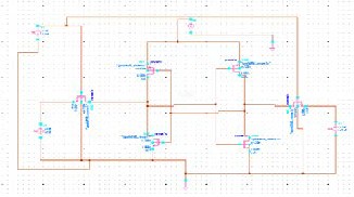
Fig1 : 6T SRAM
IJSER © 2014 http://www.ijser.org
International Journal of Scientific & Engineering Research, Volume 5, Issue 5, May-2014 298
ISSN 2229-5518
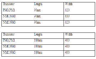
Table 1: Sizing of transistors of 6T SRAM cell
Write operation is carried out and the value to be written is applied to the bit-lines to start the writing operation. To write a 0, we would apply a 0 to the bit lines, i.e. setting –BL= 1 and BL= 0. This is similar to a causing the flip-flop to change state. A 1 is written by inverting the values of the bit lines. WL is then asserted and the value that is to be stored is latched in [3]. The main reason this works is that the bit line input-drivers are designed to be much stronger than the relatively weak transistors in the cell itself, so that they can easily override the previous state of the cross-coupled inverters [2]. Careful sizing of the transistors in an SRAM cell is needed to ensure proper operation depending on the technology being used.
In case of Read operation lets assume that the content of the memory is a 1, stored at Q. The read cycle is started by pre-charging both the bit lines to a logical 1, then asserting the word line WL, enabling both the access transistors. The second step occurs when the values stored in Q and -Q are transferred to the bit lines by leaving BL at its pre-charged value and discharging -BL through one side of transistors to a logical 0. On the BL side, the transistors on the other side pull the bit line toward VDD, a logical 1. If the content of the memory was a 0, the opposite would happen and -BL would be pulled toward 1 and BL toward
0.This justifies that the read operation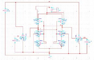
Fig2: 8T SRAM
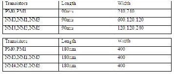
Table 2: Sizing of transistors of 8T SRAM cell
The operation of 8t SRAM cell is same as that of 6t instead here we use two additional transistors ,one each in pull down path of cross coupled inverters in order to achieve leakage power reduction.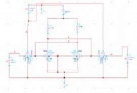
Fig3: 4T SRAM
The 4t SRAM cell comprise of four transistors and two resistors. The resistors R0 and NM2 divide the voltage between VDC and ground. When NM2 is in high impedance state, then the voltage differential falls off almost entirely at NM2, so that the connection between R0 and NM2 is at VDC[5]. In that case, NM3 is enabled and therefore in low impedance state. As a result, the voltage level between R1 and NM3 is close to ground. This in turn disables NM2, which remains in high impedance. If however NM2 is in low impedance, then the roles of NM2 and NM3 are reversed. We have seen that there exist two stable states, one with NM2 in high impedance and one with NM3 in high impedance.
Transistors NM0 and NM1 lead to two complimentary bit lines. If they are enabled, then one of the bit lines will be driven to VDC and the other one to GND. This allows reading of the SRAM cell. If one of them is driven to VDC and the other one to GND, and if then the transistors NM0 and NM1 are enabled and then disabled, the SRAM cell will stay in the state imposed on it by the bit lines. This is the write process of the SRAM cell.
IJSER © 2014 http://www.ijser.org
International Journal of Scientific & Engineering Research, Volume 5, Issue 5, May-2014 299
ISSN 2229-5518
The 4T design has a certain amount of current leakage on the lines from ground to VDC. For this reason, we can use transistors in lie of the resistors.
Table 3: Sizing of transistors of 4T SRAM cell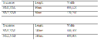
The output response of q and q’ are obtained by altering the properties such as pulse width, time period of the inputs i.e., bl, bl’ and wl.
Bit lines are connected to the access transistors when we give different pulse widths and we get four cases when wl=0 no operation takes place. When wl is enabled the operations that take place are
Table 4: Operation of 6T SRAM
Table 4: Performance characteristics of 6T 90nm
6T (90nm) | |||
VDD | POWER CONSUMPTION(W) | LEAKAGE POWER(W) | DELAY(s) |
0.8 | 6.114E-6 | 21.06E-9 | 500.6E-12 |
0.7 | 3.814E-6 | 16.96E-9 | 600.2E-12 |
0.6 | 2.106E-6 | 11.28E-9 | 2.055E-9 |
0.5 | 949.8E-9 | 5.031E-9 | 3.866E-9 |
0.4 | 293.1E-9 | 2.819E-9 | 4.317E-9 |
As the voltage value is increased, power consumption values and leakage power values are decreased whereas delay to produce output is decreased [2].
The power consumed and the leakage power values are more
when 6T is implemented using 180nm technology.
The operation of 8T SRAM cell is similar to 6t SRAM cell , the only difference is that here tow extra transistors are used to decrease the leakage power[1]. Same inputs are considered here in order to get the four cases as in table 1 i.e. No operation, Write (0), write (1) and read cases
.
Table 5: Performance characteristics of 6T in 180nm
Fig4: Transient Response of 6T SRAM
IJSER © 2014 http://www.ijser.org
International Journal of Scientific & Engineering Research, Volume 5, Issue 5, May-2014 300
ISSN 2229-5518
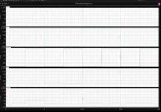
Fig5 : Transient Response of 8T SRAM Table 6: Performance characteristics of 8T in 90nm
With the scaling of voltage values power consumption and leakage power decreases whereas 8T has more speed at
0.8v as compared to lower voltage values.
Table 7: Performance characteristics of 8T in 180nm
From the above tabulated values, it can be inferred that the power consumed by the 8T SRAM cell is lower compared to that of 6T SRAM cell.
In the case 4t SRAM cell the two PMOS transistors are replaced by two resistors and because of these two resistors the power consumption and leakage power is slightly higher than the other proposed models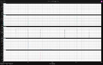
Fig6: Transient Response of 4T SRAM
From the table 8, we can conclude that the power consumption and leakage power of 4T are high compared to 6T and 8T because of the load resistors. The advantage of
4T SRAM is that it occupies lesser space than other SRAM
cells.
Table 8: Performance characteristics of 4T in 90nm
8T (180nm) | |||
VDD | POWER CONSUMPTION(W) | LEAKAGE POWER(W) | DELAY(s) |
1.8 | 143.0E-6 | 11.33E-6 | 370.0E-12 |
1.5 | 82.74E-6 | 25.6E-9 | 643.2E-12 |
1.2 | 39.4E-6 | 7.57E—9 | 2.033E-9 |
1 | 19.79E-6 | 2.14E-9 | 1.771E-9 |
0.8 | 7.30E-6 | 1.377E-9 | 1.369E-9 |
IJSER © 2014 http://www.ijser.org
International Journal of Scientific & Engineering Research, Volume 5, Issue 5, May-2014 301
ISSN 2229-5518
Table 9: Performance characteristics of 4T in 180nm
4T(180nm) | |||
VDD | POWER CONSUMPTION | LEAKAGE POWER | DELAY |
1.8 | 388.8E-6 | 353.5E-6 | 395.1E-12 |
1.5 | 261.5E-6 | 217.8E-6 | 1.486E-9 |
1.2 | 158.3E-6 | 132.1E-6 | 1.315E-9 |
1 | 102.6E-6 | 88.86E-6 | 1.834E-9 |
0.8 | 55.3E-6 | 50.24E-6 | 2.118E-9 |
We can observe that there is a huge difference in power values whereas 4T SRAM cell in 180nm is faster than 4T SRAM cell in 90 nm.
In this paper, a study on the state of SRAM cell and technologies and different performance metrics has been done. It has been analyzed that SRAM cell in 90nm technology is better than 180nm in terms of all the parameters .An efficient SRAM cell in both the aspects power consumptions and speed in terms of delay is implemented and explained.
This can be further implemented in other technology by scaling the CMOS technologies and analyzing the various parameters in order to determine the performance of SRAM cells and the same bit cells can be used to design arrays of SRAM.
The authors would like to thank Dr.I.A.Pasha, HOD, ECE Department, BVRIT and Professor Sanjay Dubey for his valuable suggestions. They also express thanks to parents, friends and colleagues.
[1] ParidhiAthe S. Dasgupta “A Comparative Study of 6T, 8T and 9T Decanano SRAM cell” 2009 IEEE Symposium on Industrial Electonics and Applications (ISIEA 2009), October
4-6, 2009, Kuala Lumpur, Malaysia.
[2] Neil H.E.Weste, David Harris and Ayan Banerjee “CMOS VLSI DESIGN – A Circuits and System perspective” Pearson eduction,Third edition, ninth impression 2009, pp. 179.
[3] Shigeki Ohbayashi, Makoto Yabuuchi, Koji Niiand, SusumuImaoka “A 65-nm SoC Embedded 6T-SRAM Designed for Manufacturability With Read and Write Operation Stabilizing Circuits” IEEE journal of solid-state circuits, Vol. 42,April 2007, pp820 – 829.
[4] International Instrumentation and Measurement Technology
Conference, Victoria, Vancouver Island, Canada, May 12-15,
2008. International Journal of Latest Trends in Engineering and Technology (IJLTET)Vol. 1 Issue 2 July 2012 51 ISSN:
2278-621X
[5] Sandeep R and Narayan T Deshpande“Design and Analysis of a New Loadless 4T SRAM Cell in Deep Submicron CMOS Technologies” Second International Conference on Emerging Trends in Engineering and Technology, ICETET-09.
[6] Rajasekhar Keerthi and Chein-in Henry Chen “Stability and
Static Noise Margin Analysis of Low-Power SRAM” I2MTC
2008 – IEEEInternational Instrumentation and Measurement Technology Conference, Victoria, Vancouver Island, Canada, May 12-15, 2008.
[7] Rashid Muhammad H “Introduction to PSpice using OrCAD
for circuits and electronics” Third edition,2009, pp. 19-25.
[8] Integrated Circuit Engineering Corporation “SRAM Technology” pp. 8.10-8.11.
[9] K.Dhanumjaya,Dr.M.N.GiriPrasad,Dr.K.Padmaraju,Dr.M.Raj a Reddy / International Journal of Engineering Research and Applications (IJERA) ISSN: 2248-9622 www.ijera.com Vol. 1, Issue 4, pp.2040-2045 2040.
[10] H. Tran. Demonstration of 5t SRAM and 6t dual-port ram cell arrays.1996 Symposium on VLSI Circuits, Digest of Technical Papers.pages 68–69, June 1996.
IJSER © 2014 http://www.ijser.org