International Journal of Scientific & Engineering Research, Volume 5, Issue 4, April-2014 508
ISSN 2229-5518
Study of multilevel inverter and analysis of three levels Inverter (FCMI)
Amarjeet.S.Pandey
![]()
Abstract— This paper deals with the study and analysis of three level flying capacitor inverter topology. These are increasingly being used in medium and high power applications due to their advantages such as low power dissipation of power switches, low harmonic contents and switching redundancy. By using the MATLAB/simulink simulation software which includes the triggering circuit, the design of FCMI was successfully done with respect to the resistive load.
Index Terms— Flying capacitor multilevel inverter(FCMI),MATLAB Simulink,
—————————— ——————————

The preliminary studies on multilevel inverters (MLI) have been Performed using three-level inverter that has been proposed by Nabae. In the study, the third level has been constituted by usingneutral point of DC line and the topol- ogy has been defined as diode clamped MLI (DC-MLI) [1,2]. In recent years, multilevel inverters have gained much at- tention in the application areas of medium voltage and high power owing to their various advantages such as lower common mode voltage, lower voltage stress on power switches, lower dv/dt ratio to supply lower harmonic con- tents in output voltage and current. Comparing two-level inverter topologies at the same power ratings, MLIs also have the advantages that the harmonic components of line- to-line voltages fed to load are reduced owing to its switch- ing frequencies. The most common MLI topologies classi- fied into three types are diode clamped MLI (DC-MLI), fly-
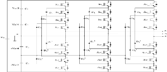
ing capacitor MLI (FC-MLI), and cascaded H-Bridge MLI (CHB-MLI). The hybrid and asymmetric hybrid inverter to- pologie have been developed according to the combination of existing MLI topologies or applying different DC bus levels respectively [6]. The basic topologies of MLIs are shown in Fig. 1. The recent applications of MLIs have a va- riety including induction machine and motor drives, active rectifiers, filters, interface of renewable energy sources, flex- ible AC transmission system (FACTS), and static compensa- tors. The diode clamped inverters, particularly the three- level structure, have a wide popularity in motor drive ap- plications besides other multilevel inverter topologies. This paper presents the multilevel inverter topologies and theircontrol methods according to existing and novel appli- cations,based on a well-surveyed literature summary. A comprehensive study has been performed on common and hybrid multilevel inverters, and the most appropriate con- trol schemesand application have been proposed accord- ing to topologies.

Electrical Department G.H.Raisoni college of Engineering Nagpur, India
IJSER © 2014 http://www.ijser.org
International Journal of Scientific & Engineering Research, Volume 5, Issue 4, April-2014 509
ISSN 2229-5518
Three major multilevel inverter structures which have been mostly applied in industrial applications have been emphasized as the diode clamped, the flying capacitor, and the cascaded Hbridge\inverters with separate DC sources. In addition to this, varioushybrid multilevel inverters have been developed by using thethree basic types mentioned above. Voltage source inverters (VSIs)are widely used in AC motor drives, AC uninterruptible power supplie(UPS), and AC power supplies with batteries, fuel cells, activeharmonic filters. VSI topologies are constituted in ac-
cord withpower demand of application areas and output voltages are eithersingle phase for power demands lower than 2 kV A or three-phasefor power demands over 2 kV A as being used in household andindustrial loads. The semi converter, half bridge and full bridgeinverters were employed for high power applica- tions in 1990s,but recently many researchers have paid much at- tention to multilevelinverters for high power and medium voltage applications[10]. Main three multilevel inverter topologies and hybridmodels of these structures have been reviewed in the fol- lowingpart of the paper by demonstrating sample models and control strategies.
The diode clamped multilevel proposed by Nabae, Takashi, and Akagi in 1981 was named as neutral point converter and was essentially a three-level diode clamped inverter as shown in
Fig. 1a. Several experimental studies and articles published about results of three, four, five and six level DC-MLIs for such uses like static VAR compensators, high voltage grid interconnections, and variable speed motor drives [9]. A three-phase five-level DCMLI topology is shown in Fig. 3. Each of the three-phase outputs
of inverter shares a common DC bus voltage that has been di- videdinto five levels over four DC bus capacitors. The capacitors havebeen subscripted from C1 to C4. The middle point of C2 and C3capacitors constitute the neutral point of inverter and output voltages have five voltage states referring to neutral point. The voltage across each capacitor is Vdc/4 and the voltage stress on eachswitching device is limited to Vdc through the clamping di- odes thathave been named as D1..3 and D1. The key components that differwith this topology from a conventional two-level in- verter areclamping diodes. To explain how the staircase voltage is synthesized, the neutral point n has been assumed as the output phase
For the five-level DC-MLI in Fig. 3, a set of four switches is ON at any given period of time and they are Sa1 to Sa4 for voltage level of
Van = Vdc/2. The second switching state shows the voltage level of Van = Vdc/4 and Sa2 to S1a 1 switches should be triggered. The
remaining switching states that constitutes 0 and negative outputs
can be seen in Table 1. The clamping diodes require different voltage
ratings for reverse voltage-blocking due to each triggered switch is only required to block a voltage level of Vdc/(m _ 1). By assuming the switches from Sa1 to Sa4 are triggered as seen
in first line of Table 1, D1 blocking diode needs to block a voltage at the rate of 3Vdc/4 that is generated by three DC bus capacitors. Since each blocking diode voltage rating is the same as the active device voltage rating, the number of diodes required for each phase will be calculated as (m _ 1) _ (m _ 2), where m repre- sents number of inverter levels.
The following equations are used to determine the required de- vice numbers to form a given level of a diode clamped MLI. If m is assumed as the number of levels,
the number of capacitors at the DC side (c) can be known by using
Eq. (1). The number of freewheeling diodes (d) per phase, and the number of clamping diodes (j) can be calculated by using Eqs. (2) and (3) respectively.![]()
(1) (2) (3)
IJSER © 2014 http://www.ijser.org
International Journal of Scientific & Engineering Research, Volume 5, Issue 4, April-2014 510
ISSN 2229-5518
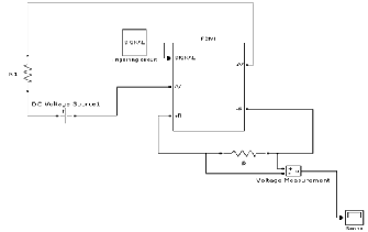
Fig.4Simulation model of the single phase three level FCMI
FCMI involves in the usage of extra capacitor clamped to
the power switches phase rail to provide the DC voltage level. This structure allows for the inverter to supply high capabilities especially during the power outages due to the redundancy in switching states provided by the clamping capacitor [3]. By assuming that the voltage rating for each of capacitor applied in the circuit is equal with the switching devices, an m-Ievel of inverter will require a total of (m - 1) x (m - 2)/2 auxiliary capacitor per phase leg in addition to (m -
1) main DC bus capacitor [3]. It is different with DCMI which for m-Ievel of this type of inverter, it is only required (m - 1) capacitors on the same voltage rating as the switching devices [3]. Thus, by taking m = 3 as an example for the number of the level in FCMI, it will give the number of auxiliary capacitor, ![]() Compared with DCMI that used N c = 2
Compared with DCMI that used N c = 2
in the circuit. Other than that, this type of multilevel inverter
also provides the switching combination redundancy that I very useful for the voltage level balancing. Basically, FCMI has redundancy at its inner voltage level which is different with DCMI. A voltage level redundancy is synthesized by two or more of valid switch combination in the circuit. It also has the capabilities to control the individual capacitor voltages in the circuit. The output voltage of the inverter can be produced
from different switching states and still produces the same output voltage level. This flexibility of the different switching states will give staircase voltage waveform at the output voltage and output current of the inverter. From FCMI configuration,
it is basically only used one DC for its operation. As been explained before, it is basically will limit the application
of the inverter itself. The FCMI will function properly when correct triggering signal is applied to the switching devices and it generates low harmonic distortion at its output.![]()
The filter is usually not used in this type of multilevel inverter.
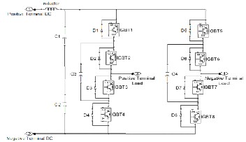
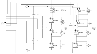
The simulation circuit of the FCMI is basically divided into three main parts. They are the triggering signal circuit, inverter circuit i.e. FCMI and also the load. The design of the singlephase three level FCMI is shown as in Figure 4. This single phase three level FCMI has eight IGBTs, thus eight signals will be required for the operation. It has two DC link capacitors at the DC side, C 1 and C2. Capacitors C3 and C4 are the clamping capacitor that will provided the variation in DC voltage level. As the number of level is increased, the amount of DC link capacitor and clamping capac- itor will also increased. One of the special feature of FCMI is it has several switching states combination for a certain value of output voltage level. Based on Zhang, Watkins and Shepherd (2002), by selecting suitable combination of switching states, all eight IGBTs can be switched on for the same duration, thus making the switching of power switches to be efficient. Eight switching states have been chosen that will give the optimum switching time for all IGBTs and this is shown in Table 2.
Each IGBTs is switched on for half of the cycle, i.e. 1800 or 0.01 s and phase shifted 450 or 2.5ms among each other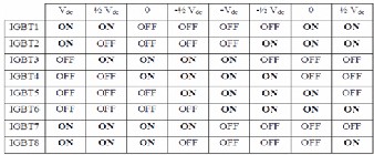
By referring to Table 1, a relationship can be obtainedamong the
IGBTs. It is found that one signal is the inverse
ofone another signal. This helps in reducing the number of ning four are the uired to be generated
IJSER © 2014 http://www.ijser.org
International Journal of Scientific & Engineering Research, Volume 5, Issue 4, April-2014 511
ISSN 2229-5518
2.3. Cascaded H-bridge multilevel inverters (CHB-MLI)
An alternative multilevel inverter topology with less power devices requirement compared to previously mentioned topologies is known as cascaded H-bridge multilevel inverter (CHB-MLI) and the topology is based on the series connection of H-bridges with separate DC sources. Since the output terminals of the H-bridges are connected in series, the DC sources must be isolated from each other. Owing to this property, CHB-MLIs have also been proposed to be used with fuel cells or photovoltaic arrays in order to achieve higher levels. The resulting AC output voltage is synthesized by the addition of the voltages generated by different H-bridge cells. Each single phase H-bridge generates three voltage levels as +Vdc, 0, -Vdc by connecting the DC source to the AC output by different combinations of four switches, SA1, SA1 1, SA 2, and SA21 as seen in first cell of Fig. 5. The CHB-MLI that is shown in Fig. 5 utilizes two separate DC sources per phase and generates an output voltage with five levels. To obtain +Vdc, SA1 and SA2switches are turned on, whereas Vdc level can be obtained by turning on the SA 2 and SA1
1. The output voltage will be 0 by turning on SA1 and SA2 switches or SA11 and SA2 switches. If n is assumed as the number of modules connected in series, m is the number of output levels in each phase as seen in Eq. (4). The switching states of a CHB-MLI (sw) can be determined by equation (5)![]()
(4) (5)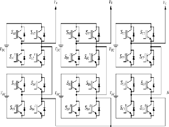
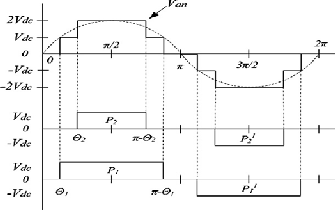
The first leg phase voltage (Van) of Fig. 5 is constituted by multi- plying Va1 and Va2 values of series connected H-bridge cells and
will generate a stepped waveform as seen in Fig. 6.
Positive output pulses are shown with P1 and P2 while the nega- tive
ones are indicated as P1 and P2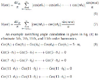
The Fourier series expansion of the general multilevel stepped
output voltage is shown in Eq. (6) and the transform is applied for Fig. 5 in Eq. (7), where n is the harmonic number of the output voltage of inverter. The switching angles that are indicated as H1 .
. .H5 in Eq.
(6) can be chosen to obtain minimum voltage harmonics and sev- eral
Since the values of Eq. (8) are non-linear, the calculations are obtained by using Newton–Raphson Iteration. The fundamental and high frequency control methods will be reviewed in the next section of the paper. CHB-MLIs have been previously designed for static VAR compensators and motor drives, but the topology
has been prepared an interface with renewable energy sources
IJSER © 2014 http://www.ijser.org
International Journal of Scientific & Engineering Research, Volume 5, Issue 4, April-2014 512
ISSN 2229-5518
due tousing separate DC sources. There are numerous studies
have beenperformed on CHB-MLIs for connecting renewable en- ergysources with AC grid and power factor correction.
Besides the three basic multilevel inverter topologies previously discussed, new MLI topologies based on the existing multilevel topologies have been proposed and classified as hybrid topolo- gies.The hybrid multilevel topologies are constituted by using combination of two basic topologies utilize the DC-MLI or
FC-MLIto replace the H-bridge as the basic module of the CHB-MLI in orderto reduce the number of the separated DC sources. The asymmetrichybrid MLIs synthesize the output voltage waveforms with reduced harmonic content [6,20]. This advantage is achieved byusing distinct voltage levels in different modules, which can generatemore levels in output voltage wave- form and reduces the THDratio, while preventing to increase the number of switching devicesand sources. Each power module of a hybrid MLI can be operated atdistinctive DC voltage and switch- ing frequency improving the efficiency and THD compensation characteristics of inverter. Nevertheless, conventional PWM strat- egies, which generates switching frequency at fundamental fre- quency are not appropriate for AHMLIs due to switching devices of the higher voltage modules, would have to operate at high fre- quencies only during some inverting instants. To achieve this control strategy, hybrid modulation methods have been proposed that provide to get higher power cells switched at low frequency and low power cells switched with high frequency [13].
The most widely used AH-MLI topologies are shown in Fig. 7 as one phase legs of three-phase applications. The diode clamped and H-bridge cascaded seven-level hybrid topology is
shown in Fig. 7a. Other seven-level hybrid topologies that are constituted by cascading flying capacitor module or H-bridges of different switching devices to basic CHB-MLI module are seen in Fig. 7bandc, respectively. The hybrid DC-MLI topology in Fig. 7a utilizes CHB-MLI’s excellent input current and output voltage property to constitute an efficient and reliable module.
On the other hand ,DC-MLI has a simple circuit, but requires a large LC output filtering motor drive applications. The hybrid FC- MLI topology obviates filtering requirements proportionally to DC-MLI, but this topologies not robust as hybrid CHB-MLI to reduce harmonic contents and about the cost of construction. The asymmetric hybrid CHB-MLI inFig. 7c uses a gate turn-off (GTO) module with an insulated-gate bipolar transistor (IGBT) H-bridge module and reveals a high voltage-blocking but a low switching
frequency capability. This trade-off can be dealt by using a hy- brid asymmetric MLI. Applying this approach to CHB-MLI topology allows reducing Fig. 7. One phase legs of three-phase asymmetric hybrid MLI topologies: (a) DC-MLI and CHB-MLI cascaded, (b) FC-MLI and CHB-MLI cascaded, (c) asymmetric hybrid CHBMLI
the number of H-bridge modules while maintaining the number of output voltage levels.
Hybrid MLIs promise significant improvements for medium voltage and high power industrial drives. Asymmetrical
multi level inverters provide minimizing the harmonic contents of output voltage without increasing the number of power devices. The use of various DC voltages in supply leads the H-MLI topol- ogies in an effort to optimize the power processing of the entire system. Thesurveyed features increase the flexibility and reliabil- ity of H-MLIs.
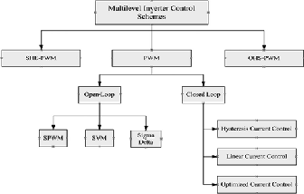
The efficiency parameters of a multilevel inverter such as switching losses and harmonic reduction are principally dependedon the modulation strategies used to control the inverter. As depicted in Fig. 2, multilevel inverter control techniques are based on fundamental and high switching fre- quency. Another widelyused popular classification for the modu- lation methods developedto control the multilevel inverters is depend upon open loop andclosed loop concepts as depicted in Fig. 8. Three main control techniques of multilevel inverters are SHE-PWM, PWM, and optimized harmonics stepped pulse width modulation (OHS–PWM).The regular PWM modulation method can be classified as openloop and closed loop owing to its control strategy. The open loopPWM techniques are SPMW, space vector PWM, sigma–delta modulation, while closed loop current control methods are defined as hysteresis, linear, and optimized current control techniques.
The modulation methods developed to control the multilevel in- verters are based on multi-carrier orders with PWM. Due to pre- defined calculations are required, SHE-PWM is not an appropri- ate solution for closed loop implementation and dynamic opera- tion in multi level inverters. Among various control schemes, the sinusoidalPWM (SPWM) is the most commonly used control scheme for the control of multilevel inverters. In SPWM, a sinus- oidal reference
waveform is compared with a triangular carrier waveform to generate switching sequences for power semiconductor in in- vertermodule [21,22].
Another fascinating control scheme is SVM as one of the most promising control methods in three-phase systems. Despite three-level SVM control is obtained by using two-level SVM, three-level mode is significantly more complex than two-level structure due to increased number of power semiconductors. As a result of this complexity, three-level SVM algorithm is Almost implemented using digital signal processors (DSPs)
or microcontroller units (MCUs) [22].
One of the most important methods to optimize control of the inverter is to select and design appropriate PWM modulation according to inverter topology. The control methods of hybrid multilevel inverters are based on multi-carrier SPWM. Fundamen- tal switching frequency methods shall be selected to reduce switching losses for high voltage modules, while multi-carrier SPWM is selected to control low voltage modules. A detailed re- view has been performed for various modulation methods in the following and a comparison list has been presented to match in- verter topologies to control methods at the end of this section.
IJSER © 2014 http://www.ijser.org
International Journal of Scientific & Engineering Research, Volume 5, Issue 4, April-2014 513
ISSN 2229-5518
The selective harmonic elimination PWM (SHE-PWM) technique is based on fundamental frequency switching theory proposed
by Patel in 1974 [14], and dependent on the elimination of defined harmonic content orders. The main idea of this method is based on defining the switching angles of harmonic orders to eliminate and obtaining the Fourier series expansion of output voltage. An example output voltage Fourier expansion of an 11- level inverter can be written as in Eq. (10).
where n defines the harmonic order at the output voltage of mul- tilevel inverter. The required switching angles to eliminate 5th,
7th, 11th, and 13th harmonic orders at fundamental switching frequency for an 11-level multilevel inverter can be calculated as given in Eq. (11voltage THD ratio, while ma defines the modula- tion index ofmodulator. Since the parameters of Eq. (11) are non- linear, the values are obtained using Newton–Raphson Iterations. The switching angles can be obtained at the values of h1 = 6.57,
h2 = 18.94_,h3 = 27.18_, h4 = 45.14_ and h5 = 62.24_ by
assuming ma as 0.8 andsolving with Newton–Raphson Iteration. In the application of SHE-PWM, possible switching angles are calculated previouslyand saved to look-up tables in an independent memory or microprocessor.
The main defect of SHE-PWM is the requirement of calculations
to determine switching angles as in fundamental frequency switching method. However, Newton–Raphson Iteration is able to solve an equation similar to Eq. (11), the initial values are based on guesses or assumes and the results will not be at accurate val- ues. In addition to this, increased DC sources or switching angles will prevent to obtain the most accurate solution.
SPWM technique is one of the most popular modulation Techniques among the others applied in power switching invert- ers.
InSPWM, a sinusoidal reference voltage waveform is compared witha triangular carrier waveform to generate gate signals for the switches of inverter. Power dissipation is one of the most important issues in high power applications. The fundamental frequency SPWM control method was proposed to minimize the switching losses.The multi-carrier SPWM control methods also have beenimplemented to increase the performance of multilevel inverters and have been classified according to vertical or horizontal arrangements of carrier signal. The vertical
carrier distribution techniques are defined as Phase Dissipation (PD), Phase Opposition Dissipation (POD), and Alternative Phase Opposition Dissipation(APOD),
while horizontal arrangement is known as phase shift- ed(PS)control technique.In fact PS-PWM is only useful for cascad- ed H-bridges andflying capacitors, while PD-PWM is more useful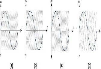
for NPC [12,18].
have been illustrated in Fig. 9, respectively. The sinusoidal SPWM is the most widely used PWM control method due to many ad- vantages including easy implementation, lower harmonic outputs according to other techniques, and low switching losses. In SPWMcontrol, a high frequency triangular carrier signal is com- pared witha low frequency sinusoidal modulating signal in an analog or logiccomparator devices. The frequency of modulating sinusoidal signaldefines the desired line voltage frequency at the inverter output[23].
IJSER © 2014 http://www.ijser.org
International Journal of Scientific & Engineering Research, Volume 5, Issue 4, April-2014 514
ISSN 2229-5518
Most applications of three-phase voltage source PWM inverters such as motor drives, active filters, and static VAR compensators require a control structure comprising an internal current feed- backloop. Multilevel inverter systems also utilizes photovoltaic (PV)sources or wind generators to integrate renewable energy sourcesto grid. The performance of the inverter systems which are suppliedwith DC sources mentioned before largely depends on
the quality of the applied current control strategy. Numerous studies have been performed to reduce harmonic contents using current control for active power filter or PV and wind generator inter connection to grid applications of MLIs.
The applied current control techniques are mostly focused on hysteresis current control(HCC) and
linear current control (LCC) [24].
The hysteresis modulation is a feedback current control method where the load current tracks the reference current within a hys- teresis band in nonlinear load application of an MLI. Fig. 10a shows the block diagram of a hysteresis control of an H-bridge and Fig. 10b shows the operation principle of the hysteresis mod- ulation.The controller generates the sinusoidal reference current ofdesired magnitude and frequency that is compared with the actualline current. If the current exceeds the upper limit of the hysteresisband, the next higher voltage level should be selected to attempt toforce the current error towards zero. However, the new invertervoltage level may not be sufficient to return the current error tozero and inverter should switch to next higher voltage level untilthe correct voltage level is selected. As a result, the cur- rent getsback into the hysteresis band, and the actual current is forced totrack the reference current within the hysteresis band. Three hysteresis controllers which are used to implement the cor- rect voltage level selection are defined as double offset band three level, double band three level, and time-based three level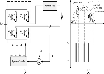
hysteresis controllers [24].
The most common multilevel inverter topologies and control schemes have been reviewed in this paper. As mentioned in Section1, the multilevel concept has been introduced with a Diode clamped topology in 1980s by Nabae. MLIs are
increasingly being used in medium voltage and high
power applications owing to numerous advantages such as low power dissipation due to reducingthe voltage stress on switching devices and minimizing theharmonic contents
at the output of the inverter.
The selected control scheme for an MLI determines the affectivity on harmonic elimination, while generating the ideal output voltage. The applications of MLIs including induction machine and motor drives, active filters, renewable energy sources interconnection to grid, flexible AC transmission systems (FACTS), and static compensa-
tors(STATCOM) have been widely used in industrial applications. Although the variety of MLI applications, there are several limita- tions have been discussed for topologies and control schemes.
DC-MLIs,especially three-level structure, have a wide popularity in motor drive applications besides other multilevel topologies due to reducing THD with robust control of SHE-PWM
control scheme.
However, it would be a restriction of complexity and
pre-define switching angles when the level exceeds the three. The SPWM and SVM modulation techniques succeed this limitation of DC-MLI for higher level topologies. Other applications of DC-MLI can be defined as active filters
and STATCOM in high voltage grid interconnections. Table 3 illustrates the most appropriate control schemes
with application matching according to selected multi level inverter topology.
The sign of bolded check means the proper matching between topology and control scheme or topology and application. The plain checks have been used to emphasize that there are some studies given in the literature about these applications but does not provide proper solutions. The bolded double check shows the most appropriate selection, while the cross defines
the undesirable latching about harmonic reducing or affectivity issues.
The DCMLIs are efficient in fundamental frequency Switching applications such SHE-PWM and SVM, but the SVM will cause to an increment on voltage and current THD in the increased number of clamping diode conditions.
The FC-MLI topology that has been introduced
in 1992 is similar to DC-MLI except utilizing DC side capacitors instead of clamping diodes in a ladder form.
The FC-MLI is the unique topology that requires the most Switching and auxiliary devices to generate a staircase output voltage. The increment of level will cause to increase auxiliary capacitor number and restrain the accurate charging and dis- chargingcontrol of capacitors, hence designer will be encountered
IJSER © 2014 http://www.ijser.org
International Journal of Scientific & Engineering Research, Volume 5, Issue 4, April-2014 515
ISSN 2229-5518
withthe requirement of a pre-charge controller system. Although thesedisadvantages, the most important advantages of FC-MLI topologyare preventing the filter demand, and controlling the active andreactive power flow besides phase redundancies. The FC-MLItopology is mostly used in motor drive and active filter applicationswith SHE-PWM or phase shifted PWM control meth- ods.The CHB-MLI has the least components for a given number oflevels according to topologies discussed before. The CHB-MLI topology consists of a series of H-bridge cells to synthesize a desired voltage from SDCSs which may be obtained from bat- teriesor fuel cells. All these properties of cascade inverters allow usingvarious pulse width modulation (PWM) strategies to control theinverter accurately. CHB-MLIs have been previously designed forstatic VAR compensators and motor drives, but the topology
hasbeen prepared an interface with renewable energy sources due tousing separate DC sources. There are numerous studies have beenperformed on CHB-MLIs for connecting renewable energy sourceswith grid and power factor correction. The SPWM control schemeis mostly being used in the control of CHB-MLI due to simplifieddesign considerations according to SVM.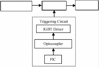
4.Design and development of FCMI Simulation model
DC Supply FCMI LOAD
The simulation model of three levels FCMI was developed usimg MATLAB/Simulink simulation software.Fig.3.shows the block dia- gram of single phase 3 level FCMI.
Fig.4Simulation model of the single phase three level FCMI
The simulation circuit of the FCMI is basically divided into three main parts. They are the triggering signal circuit, inverter circuit i.e. FCMI and also the load. The design of the single phase three level FCMI is shown as in Figure 4. This single phase three level FCMI has eight IGBTs, thus eight signals will be required for the operation. It has two DC link capacitors at the DC side, C 1 and C2. Capacitors C3 and C4 are the clamping capacitor that will provided the variation in DC voltage level. As the number of level is increased, the amount of DC link capacitor and clamping capac- itor will alsoincreased. One of the special feature of FCMI is it has several switching states combination for a certain value of output voltage level. Based on Zhang, Watkins and Shepherd (2002), by selecting suitable combination of switching states, all eight IGBTs can be switched on for the same duration, thus making the switch- ing of power switches to be efficient[7].
Eight switching states have been chosen that will give the opti- mum switching time for all IGBTs and this is shown in Table
2.Each IGBTs is switched on for half of the cycle, i.e. 1800 or 0.01
s and phase shifted 450 or 2.5ms among each other
IJSER © 2014 http://www.ijser.org
International Journal of Scientific & Engineering Research, Volume 5, Issue 4, April-2014 516
ISSN 2229-5518
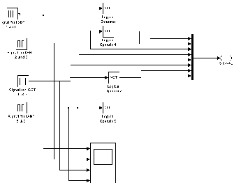
The simulation model of triggering circuit is shown in fig.5
The figure consists of signal triggering and NOT logical operator.
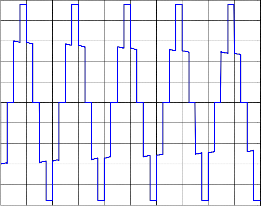
Fig.9.Waveform of output voltage,VLL(V) against time,t(s)
Considering the complete simulation model in fig.6 with the spec-
100
80
60
40
20
0
-20
-40
-60
-80
-100
0 0.01 0.02 0.03 0.04 0.05 0.06 0.07 0.08 0.09 0.1
Time(sec)
ification of Considering Vdc=12Volt, load Resistance =10 Ω,DC link Capacitor (C1,C2=0.01uFarad) with multiple switching trig- gering technique.
5. Result:-
Based on the timing diagram and by referring to Table 1, a rela- tionship can be obtainedamong the IGBTs. It is found that one signal is the inverse of one another signal. This helps in reducing the number of switching signals to four, and the remaining four are the
inverse. As shown in fig.8 the triggering of IGBT 4,IGBT 3,IGBT
6,IGBT 5 MATLAB software by applying the parameter of every
45(degree) or 2.5 msas shown in fig.8.The output signals from PIC then passed optocoupler and IGBT drivers.
As shown in fig.9. the Waveform of output voltage,VLL(V) with
respect to the source input voltage of 100 V(dc).
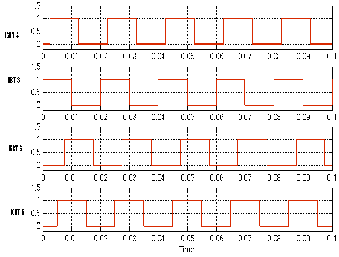
Fig.8.Timing diagram of triggering circuit for FCMI
6. Conclusions:-
![]()
This paper deals with the study and analysis of three level flying capacitor inverter topology. These are increasingly be- ing used in medium and high power applications due to their advantages such as low power dissipation of power switches, low harmonic contents and switching redundancy. By using the MATLAB/simulink simulation software which includes the triggering circuit, the design of FCMI was successfully done with respect to the resistive loadBased on the survey of conventional multilevel inverter topologies given in the previous sections, general and asymmetricallyconstituted H-MLIs have been also reviewed in this paper. Manynew hybrid topologies can be designed through the combinationsof three main MLI topolo- gies. Besides the combination of topologies,the trade-offs in MLI structures can be dealt by using AH-MLIsthat is formed using different DC source levels in inverter cells.Nevertheless, conven- tional PWM strategies that generate switchingfrequency at fun- damental frequency are not appropriate forAH-MLIs due to switching devices of the higher voltage moduleswould have to operate at high frequencies only during someinverting instants.
To achieve this control strategy, hybrid modulationmethods have been proposed that provide to get higher powercells switched at low frequency and low power cells switched withhigh frequency.
7. References
[1] Colak I et al. Review of multilevel voltage source inverter
IJSER © 2014 http://www.ijser.org
International Journal of Scientific & Engineering Research, Volume 5, Issue 4, April-2014 517
ISSN 2229-5518
topologies and control schemes Ilhami Colak a, Ersan Kabalci b,⇑ , Ramazan Bayindir aDepartment of Electrical Education, 2010), doi:10.1016/j.enconman.2010.09.006
[2] Nabae A, Takashi I, Akagi H. A new neutral-point clamped
PWM inverter. IEEE Trans Ind Appl 1981;17:518–23.
[3] “Simulation & construction of single phase FCMI”Nashiren
F.Mailah,2010 IEEE Conference on R&D,13-14 Dec 2o1o
[4] Bose BK. Modern power electronics and AC drives. NJ, USA: Prentice Hall; 2001.
[5] Mohan N, Undeland TM, Robbins WP. Power electronics- converters, application and design. New York: John Wiley & Sons Inc.; 1995.
[6] Rodriguez J, Lai S, Peng FZ. Multilevel inverters: a survey of topologies, control and applications. IEEE Trans Power Electron
2002;49:724–38..
[7] Su Gui-Jia. Multilevel DC-link inverter. IEEE Trans Ind Appl
2005;41:848–54.
[8] Lin BR. A novel control scheme for the multilevel rectifi- er/inverter. Taylor and Francis Int J Electron 2001;88:225–47.
[9] Lopez O, Alvarez J, Gandoy JS, Freijedo FD. Multilevel multi-
phase space vector PWM algorithm. IEEE Trans Ind Electron
2008;55:1933–42
[10] . Lai JS, Peng FZ. Multilevel converters: a new breed of power converters. IEEE Trans Ind Appl 1996;30:509–51.
[11] Peng FZ, McKeever JW, Adams DJ. Cascade multilevel in- verters for utility applications. In: Proceedings of 23rd interna- tional conference on industrial elect. control and inst, New Orle- ans (USA); 1997.
[12] Maynard TA, Foch H. Multi-level conversion: high voltage choppers and voltage-source inverters. In: Proceedings of IEEE power electronics specialists conference, Toledo (Spain); 1992. [13] Veenstra M, Rufer A. Control of a hybrid asymmetric multi- level inverter for competitive medium-voltage industrial drives. IEEE Trans Ind Appl2003; 41:655–64.
[14] Patel HS, Hoft RG. Generalized harmonic elimination and voltage control in thyristor converters: part i – harmonic elimina- tion. IEEE Trans Ind Appl 1973;9:310–7.
[15] Ishida T, Matsuse K, Sugita K, Huang L, Sasagawa K. DC voltage control strategy for a five-level converter. IEEE Trans Power Electron 2000;15: 508–15.
[16] Zare F, Ledwich G. A hysteresis current control for single- phase multilevel voltage source inverters: PLD implementation. IEEE Trans Power Electron 2002;17:731–8.
[17] Mohan N, Undeland TM, Robbins WP. Power electronics-
converters, and design. New York: John Wiley & Sons Inc.; 1995. [18] L., Zhang, S.J., Watkins, w., Shepherd, Analysis and Control of A Multi-level Flying Capacitor Inverter, Power Electronics Congress 2002, Technical Proceedings, CIEP 2002, VIII IEEE In- ternational, 2002, pp. 66-71
[19] Peng FZ, McKeever JW, Adams DJ. Cascade multilevel in- verters for utility applications. In: Proceedings of 23rd interna- tional conference on industrial elect. control and inst, New Orle- ans (USA); 1997.
[20] Manjrekar MD, Lipo TA. A hybrid multilevel inverter topol- ogy for drive applications. In: Proceedings of IEEE applied power elec conference; 1998.
[21] Jinghua Z, Zhengxi L. Research on hybrid modulation strate- gies based ongeneral hybrid topology of multilevel inverter. In: Proceedings of int symppower elect, elec drives, motion, Ischia
(Italy); 2008.
[22] Kouro S, Rebolledo J, Rodriguez J. Reduced switching- frequency-modulation algorithm for high-power multilevel in- verters. IEEE Trans Ind Electron 2007;54:2894–901.
[23] Ismail B, Taib S, Saad RM, Isa M, Hadzer CM. Development of a single phase SPWM microcontroller-based inverter. In:Proceedings of 1st international power and energy conference PECon 2006, Putraja (Malaysia); 2006.
[24] Loh PC, Bode GH, Holmes DG, Lipo TA. A time-based hyste- resis current regulation strategy for single-phase multilevel in- verters. IEEE Trans Ind. Appl 2003;39:883–92.
IJSER © 2014 http://www.ijser.org