International Journal of Scientific & Engineering Research, Volume 4, Issue 7, July-2013 2541
ISSN 2229-5518
Disha S. Aherrao#, S.W.Varade*
Abstract— Power consumption is the key issue for implementing serial I/O receivers based on ADCs in high speed applications. This paper presents an ADC-based serial link receiver that uses 45nm technology. The receiver is based on a low power design of Analog to Digital converter, using 45nm technology thus lowering the power consumption of overall system. This paper proposes a low-gain mixed-mode or analog mode pre-filtering. The ADC- based receiver would pre-shape the signal and thus could reduce amount of Digital Signal Processing in it. Performance analysis has been done to show how performance and power efficiency can dramatically improved using non-uniform quantization levels. This paper is using Tanner tool 13.0 for the simulation of the proposed design. It can be seen that the modules used in the proposed ADC lowers the power consumption from the simulation results.
Index Terms— Serial link receiver, digital equalizer, Sequence detector, Analog-to-Digital Converter
In high speed applications, using ADC based receivers power consumption remains the main problem. Since last few decade, the wireless communication industry has experienced a drastic improvement .Typical smart communication device should include all radio and internet services. A smart communication device should not only be capable of meeting all such requirements but has to be highly flexible that the device be able to reconfigure radio transmitters and receivers as per requirement. Also such radio modules should be minimizing BER as its main function to maximize the receiver voltage margin.
This technique enables near-optical BER performance and requires almost no additional hardware compared to the traditional adaptation approach. Along with this, the device should satisfy minimal cost and energy requirement. a common trend in digital communication has increased the use of Digital Signal Processing .There has been a growing interest in in-corporating CMOS Analog-to- Digital converters (ADCs) as frontend of high speed serializers/deserializers(Ser/Des) and Electronic Dispersion Compensation (EDC) of optical links.Since the resolution and speed are achieving low power dissipationis a big challenge,so that I/O links can be intergrated in large ASICs.
This paper focuses on design of low power ADC module
for serial link Receiver, which would contain a low gain
Analog Front End (AFE) to pre-shape the signal. This work
also introduces adopted variable-references for ADC that can compensate for undesired non-linearity of frontend, mismatch between interleaving paths and optimally locate the slicing level to maximize the voltage margin for receiver signal.
Also, a new adaptation strategy of I/O link equalizer and clock Data Recovery (CDR) is presented. This is based on minimizing the receiver voltage margin.
Recently, the ADC based receiver has given a good comparable power/performance which uses the data rate around 10Gbps.This paper proposes a low-gain mixed- mode or analog mode pre-filtering. This ADC- based receiver would pre-shape the signal and thus could reduce amount of Digital Signal Processing in it. If there is a requirement for the ease of programmability, extensively for different channel characteristics and robustness to process variations, ADC-based receiver is among the best choices. For ADC resolution no. of conversion levels depends on the link characteristics.
In pipeline mode, more highly interleaved designs using
pipelined ADC can reach a higher no. of bits for same i/p
capacitance. The references levels are not fully programmable and hence cannot be used for loop-unrolled architecture benefits.
Design trade-offs and power considerations in concern with timing recovery have some drawbacks:
1. With ISI the phase information has a poor distribution.
2. The binary data are decided after a long latency which dramatically reduce the bandwidth of loop and incur large jitter and less phase tracking.
Any receiver circuitry adopts a simple frontend circuitry which is meant for low gain and high loss serial link application, pre-filtering is done using this simple frontend
IJSER © 2013 http://www.ijser.org
International Journal of Scientific & Engineering Research, Volume 4, Issue 7, July-2013 2542
ISSN 2229-5518
circuitry. A continuous-time linear equalizer (CTLE) a very building for receiver pre-filtering, in a mixed mode receiver
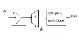
Fig. 1 General ADC-based receiver
Figure 1: show a general ADC-based receiver architecture which comprises of a HPF/FIR filter whose input in turn is fed to digital equalizer/sequence detector.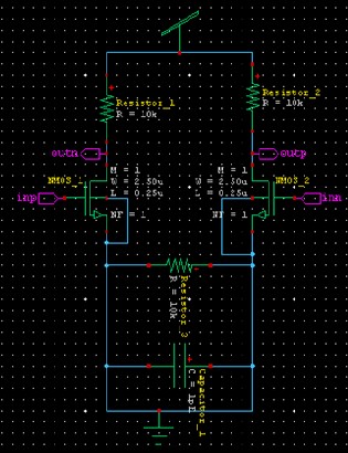
A CTLE performs basically two main functions; it contains variable DC gain to adjust received signal swing and variable high frequency boosting to provide equalization This CTLE block is used to pre-shape the signal. Also sometimes a variable gain amplifier is used to adjust signal swing. This adjustment of signal swing would properly drive ADC [6].
Fig . 2 Circuit implementation of HPF
The Figure 2 shows the actual circuit implementation of actual HPF which is required for pre-processing the signal for ADC block. Before being fed to serial link receiver, signal is fed to HPF block, which is a pre-processing block of power optimized serial link receiver. This is the very first component in AFE, which is continuous-time HPF (high pass filter) and it is realized by three CML stages with variable degeneration resistors and capacitors. Here, it has total three stages out of which first two stages are used to provide a wide tunable range of both DC and high frequency boosting. The third stage is used to drive 300 fF loading of interleaved T/H circuitry. The HPF circuitry used here has a great advantage in power consumption i.e. it requires very less power, which is the main aim of proposed paper.
The HPF is to apply power-efficient receiver pre-filtering
which consumes only 6 mW in 1.1V supply.
Optional FIR can also be implemented with a little
power cost when combined Sample-and –Hold or Track-
and -Hold circuit of ADC. By combining HPF and FIR, a
good equalization is achieved. Here AFE can perform more than 10dB equalization. The equalization leads to around 1-
2 bit saving in the required ADC resolution [7]. As the sampling speeds and input bandwidths are continuously increased, the circuits within the ADC are required to
perform faster and maintain certain performance. This becomes difficult to achieve since the performance degrades at high-speeds and affects the dynamic range of ADC.
IJSER © 2013 http://www.ijser.org
International Journal of Scientific & Engineering Research, Volume 4, Issue 7, July-2013 2543
ISSN 2229-5518
0.5 | 0 | 5 |
0.6 | 0.1 | 5 |
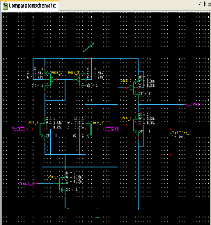
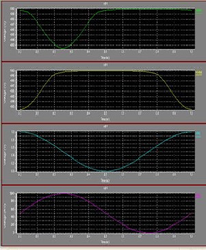
Figure 3 represents HPF output. By taking various voltage values and ranges, we can observe that for lower frequencies, the simulation is distorted and not ideal. (For about 100MHz). But as the frequency ranges are increased, the waveforms are nearly ideal. (Passes 500MHz and above). The waveforms are found to be ideal till 1GHz. The waveform shown above gives the simulation results obtained from .sp files in T-spice. These are showing the outputs.
Fig 3 Waveforms for HPF
TABLE 1.
SIMULATION RESULTS FOR HPF
TABLE 2.
SIMULATION RESULTS FOR HPF
Fig 4 Schematic of comparator
Figure 4 is the schematic of comparator, which is the 2nd module of the proposed design. This module has basically two inputs VinP and VinN. The comparator compares the two input values of VinP and VinN. When input value VinP is greater than VinN, then VOut is less because at the output there is implementation of inverter. Similarly when input VinP is less then VinN the VOut of the comparator is more.
The ADC which is introduced in this paper requires eight such comparators if we use 8 bit data. So a cascade of
eight such comparators is the next step .Fig.5 shows the schematic of final ADC.
IJSER © 2013 http://www.ijser.org
International Journal of Scientific & Engineering Research, Volume 4, Issue 7, July-2013 2544
ISSN 2229-5518
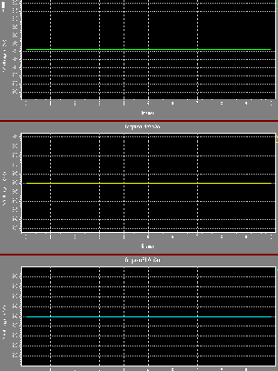
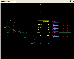
Fig. 5 ADC schematic
TABLE 3.
SIMULATION RESULTS FOR COMPARATOR
V(VinP) | 2.40V |
V(VinN) | 2.60V |
V(Vout) | 2.90V |
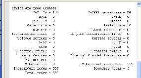
Fig 6 Waveforms for comparator.
The above Fig. 6 shows the waveforms of the comparator generated form the T-spice. Similarly Figure 7 shows the simulation results generated from the T-spice window,output of the final ADC module i.e. shown in Figure 5.
Fig 7 Device and node counts 
Fig 8 simulation result
I. PERFORMANCE COMPARISON
The proposed receiver operates at 10Gb/s rate and consumes 83uW of power. The table given below shows
IJSER © 2013 http://www.ijser.org
International Journal of Scientific & Engineering Research, Volume 4, Issue 7, July-2013 2545
ISSN 2229-5518
performance comparison on the basis of work of various authors.
TABLE 4.
PERFORMANCE COMPARISON OF HIGH SPEED SERIAL LINK RECEIVERS
This work uses 45nm technology with 10Gbps data rate. The receiver power consumption is observed to be reduced to 83uW.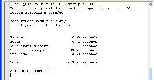
Figure 9:output window
Figure 9 shows the output window showing that the power consumption is 83.28uW.
This paper presents design & Simulation of High Speed, Low Powered ADC using Tanner tool 13.0 for Serial link Receiver. All modules has been implemented i.e. the HPF
and the comparator, threshold device for Serial link Receiver. From the simulation results it has been observed that the modules used in the proposed ADC lowers the power consumption using 45nm technology. After certain calculations it has been observed that the receiver power is lowered to 83uW.This is drastically lowering of receiver power.
[1] E-Hung chen,member IEEE,Ramy Yousry,and Chih-Kong Ken Yang,Fellow,IEEE, “Power optimized ADC based serial link Receiver”, IEEE J.Solid state Circuits ,vol.47,NO.4,april2012.
[2] M. Ramezani, M. Abdalla, A. Shoval,M. Van Ierssel, A. Rezayee, A.
McLaren, C. Holdenried, J. Pham, E. So, D. Cassan, and S. Sadr, “An
8.4 mW/Gb/s 4-lane 48 Gb/s multi-standard-compliant transceiver in
40 nm digital CMOS technology” , in IEEE Int. Solid-State Circuits
Conf. Digest of Tech. Papers (ISSCC), Feb. 20–24, 2011, pp. 352–354.
[3] G. Balamurugan, J. Kennedy, G. Banerjee, J. E. Jaussi, M. Mansuri, F.O’Mahony, B. Casper, and R. Mooney, “A scalable 5–15 Gbps, 14–75 mW low-power I/O transceiver in 65 nm CMOS” ,IEEE J. Solid-State Circuits, vol. 43, no. 4, pp. 1010–1019, Apr. 2008.
[4] Y. Hidaka, T. Horie, Y. Koyanagi, T. Miyoshi, H. Osone, S. Parikh,S.
Reddy, T. Shibuya, Y. Umezawa, and W. W. Walker, “A 4-channel,10.3
Gb/s transceiver with adaptive phase equalizer for 4-to-41 dB loss PCB
channel”, in IEEE Int. Solid-State Circuits Conf. Digest of Tech.Papers,
ISSCC, Feb. 20–24, 2011, pp. 346–348.
[5] M. Harwood, N. Warke, R. Simpson, T. Leslie,A. Amerasekera, S.Batty ,
D. Colman, E. Carr, V.Gopinathan, S.hubbins, P. Hunt, A. Joy, P.Khandelwal, B.Killips, T.Krause ,S. Lytollis, A.Pickening, M. Saxton, D.Sebastio, G. Swanson ,A. Szezepanek, T. Ward, J. Williams,and T. Willwerth,”A 12.5Gb/s SerDes in 65nmCMOS using baud-rate ADC with digital receiver equalization and clock recovery,”in IEEE Int.Solid State Circuits Conf.Digest of Tech.Papers,2007,pp. 436-591.
[6] O.E. Agazzi,M. R. Hueda,D.E. Crivelli,H. S. Carrer, A. Nazemi,G. Luna,
F. Ramos, R. Lopez, C. Grace, B. Kobeissy, C. Abidin, M. Kazemi,M. Kargar,C. Marquez, S. Ramprasad, F.Bollo, V. Posse, S. Wang, G.Asmanis,G.Eaton , N. Swenson, T. Lindsay, and P. Voois,”A 90nm CMOS DSP MLSD transceiver with integrated AFE electronic dispersion compensation of multimode optical fibers at 10Gb/s”,IEEE J.Solid State Circuits,vol.43,no.12,pp.2939-2957,Dec.2008
[7] E.-H. Chen and C.-K. K. Yang, “ADC-based serial I/O receivers,”
IEEE Trans. Circuits Syst. I: Reg. Papers, vol. 57, no. 9, pp.
2248–2258, Sep. 2010.
IJSER © 2013 http://www.ijser.org