International Journal of Scientific & Engineering Research, Volume 4, Issue 6, June-2013 840
ISSN 2229-5518
Sense amplifier approach for high speed SRAM Cell
Er. Robin Mehta, Er. Amit Kumar
Abstract—In this paper a high speed hybrid current mode sense amplifier is presented. Sense amplifier is the most important component of SRAM cell used to sense stored data. Sense amplifiers are used to read the contents of SRAM cells. Sense amplifiers perform amplification, delay reduction and power reduction. Earlier voltage mode sense amplifiers are used to sense the data from bitlines. But with increase in bitline capacitance delay increases in voltage mode sense amplifier. So hybrid current mode sense amplifier is a new approach of sensing data with minimum delay and power dissipation. This paper explores the design and analysis of hybrid current mode sense amplifier. The simulation is carried out at 1.8V / 0.18µm technology using tanner (13.0 Version) tool. The results are compared with voltage mode sense amplifier.
Index Terms—Bitline capaciatance, Delay reduction, Power dissipation, Sense amplifiers, SRAM cell, Tanner EDA, 0.18µm technology
1 INTRODUCTION
—————————— ——————————
TODAY with increase in advancement the need of
battery powered devices has been increased. According to
Moore’s law the number of transistors on a chip roughly
doubles every two years. As a result the scale gets smaller and smaller. So the ever-increasing levels of on-chip integration in the recent decades have led to increase in the densities of integrated circuits by decreasing the device geometries. Other major factor behind the low power[7] design is increased market of mobile devices and battery powered portable electronic system is creating demands for the chips that consume the smallest amount of power such as PDA, Tabs and smart cards. Static RAM consists of almost 90% of Very large Scale Integrated Circuits. The power consumption [3] and speed of SRAMs are important issue that has lead to multiple designs with the purpose of minimizing the power consumption during both reading and writing operation. In a circuit mainly three components are responsible for power dissipation which are dynamic power, short circuit power and static power [4]. The sense amplifier [1], [2] plays an important role in delay [8] reduction and low power dissipation. In my paper I compare the voltage mode sense amplifier circuit with hybrid current mode sense amplifier circuit.
————————————————
• Er. Robin Mehta is currently currently pursuing masters degree program in Microelectronics engineering from BMSCE, Muktsar, Punjab (India) PH-094683-33878. E-mail: robinmehta66@gmail.com
• Er. Amit Kumar working as an Asst. Professor in ECE Deptt. in BMSCE, Muktsar, Punjab(India), PH-098557-85410.
E-mail: amitkumar.sgnr@gmail.com
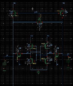
2 6T SRAM CELL WITH PRECHARGED CIRCUIT
The memory cell is the basic building block of any static memory system. As shown in fig 1, a conventional six transistor (6T) static memory cell [5].
The circuit is a flip-flop comprising two cross-coupled
inverters and two access transistors. The access transistors
are turned on when the word line (WL) is asserted and
connect the memory cell to the column bit lines (BL or
BLB). They act as transmission gates allowing bidirectional
current flow between the flip flop and the two bit lines. Both the bit lines carry complementary data and connect all the memory cells in a single column. The word line should be high to connect the memory cell and the bit lines and for performing a read or write operation on the memory cell. Each memory cell has two bit lines is used to distinguish between a memory read or write operation [6].
Fig. 1 6T SRAM Precharged Circuit
IJSER © 2013 http://w w w .ijser.org
International Journal of Scientific & Engineering Research, Volume 4, Issue 6, June-2013 841
ISSN 2229-5518
3 VOLTAGE MODE SENSE AMPLIFIER
In SRAM memory architecture sense amplifier is the important part of the circuit which amplifies the voltage or current difference on the bitlines. In voltage mode sense amplifier voltage level is amplified. In the circuit shown input voltage to voltage mode sense amplifier is bitline voltage given to two NMOS transistors NMOS_7 and NMOS_8. A common clock signal is given to the transistor NMOS_9, PMOS_8 and PMOS_9. Four transistors PMOS_6, PMOS_7, NMOS_5 and NMOS_6 form two inverter circuits. The output is taken from out and outb. The separate voltage supply source of 1.8V is used for voltage mode sense amplifier circuit.
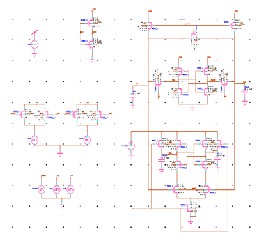
Fig. 2 6T with Voltage mode sense amplifier
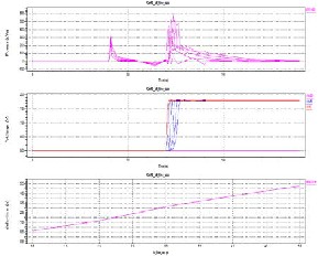
3.1 Simulation Results A clock pulse vs is given as shown in fig 3, which is low for the duration of 70ns and high up to 180ns. The above results are shown for power dissipation [9] for the bitline capacitance of 1pf and output capacitance of 0.1 pf. The curve for total power dissipated and delay time is shown in fig. with variable bitline capacitance.
At output capacitance = 1pf
Bitline capacitance variation | Delay (seconds) | Power Dissipation (watts) |
1e-012 | 6.5359e-010 | 5.988760e-005 |
2e-012 | 1.6586e-009 | 1.456161e-004 |
3e-012 | 3.1304e-009 | 1.916076e-004 |
4e-012 | 4.2523e-009 | 2.025226e-004 |
5e-012 | 5.2972e-009 | 2.040857e-004 |
Table 1 Results of VMSA
The result of Voltage mode sense amplifier shows that with bitline capacitance increase delay time is increasing and power dissipation is also increasing.
4 HYBRID CURRENT MODE SENSE AMPLIFIER
In a Hybrid Sense amplifier both current and voltage sensing techniques [10], [11] are used which makes it a better selection than a conventional current or voltage sense amplifiers. The schematic of hybrid sense amplifier is shown in fig 4.
Fig. 4 6T with Hybrid current mode sense amplifier
Fig. 3 W- Edit result of 6T with VMSA
4.1 Simulation Results
The simulation results for hybrid current mode sense amplifier are shown in fig. 5.
IJSER © 2013 http://w w w .ijser.org
International Journal of Scientific & Engineering Research, Volume 4, Issue 6, June-2013 842
ISSN 2229-5518
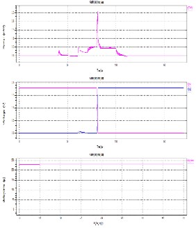
Fig. 5 W- Edit result of 6T with HCMSA At output capacitance = 0.1pf
Table 1 Results of HCMSA
From the simulation table it is observed that delay is constant for hybrid current mode sense amplifier.
5 RESULT COMPARISON
| VMSA | HCMSA |
Bitline Capacitan ce | Delay (secon ds) | Average Power Dissipatio n | Delay (seconds ) | Average Power Dissipatio n |
1e-012 | 6.5359 e-010 | 5.988760e -005 | 2.2955e- 010 | 3.261363e- 004 |
2e-012 | 1.6586 e-009 | 1.456161e -004 | 2.3102e- 010 | 3.267157e- 004 |
3e-012 | 3.1304 e-009 | 1.916076e -004 | 2.3168e- 010 | 3.274058e- 004 |
4e-012 | 4.2523 e-009 | 2.025226e -004 | 2.3204e- 010 | 3.280068e- 004 |
5e-012 | 5.2972 e-009 | 2.040857e -004 | 2.3228e- 010 | 3.283856e- 004 |
Table 1 Result Comparison of VMSA & HCMSA
6 CONCLUSION
In my paper a low power 6T SRAM cell with voltage mode sense amplifier and then with hybrid current mode sense amplifier is designed using Tanner 13.0 at 0.18 µm technology and simulation results are shown for delay and power dissipation. The simulation result shows that delay increases with bitline capacitance in case of voltage mode sense amplifier and almost constant in hybrid mode sense amplifier. The hybrid mode sense amplifier shows minimum delay of 0.23ns. The power dissipation also increases with increase in bitline capacitance for voltage mode sense amplifier and almost constant and hybrid mode. But voltage mode sense amplifier shows minimum power dissipation of 59 µW at bitline capacitance of 1pf.
REFERENCES
[1] Anh-Tuan, D. et al, “Hybrid-Mode SRAM Sense Amplifiers: New Approach on Transistor Sizing”, IEEE TRANSACTIONS ON CIRCUITS AND SYSTEMS—II: EXPRESS BRIEFS, VOL. 55, NO. 10, OCTOBER 2008
[2] Kumar, S. et al., “Comparative Study Of Different Sense Amplifiers In Submicron Cmos Technology”, INTERNATIONAL JOURNAL OF ADVANCES IN ENGINEERING & TECHNOLOGY. IJAET ISSN: 2231-1963, NOV 2011
[3] Wang, M.C., “Low Power Dual Word Line 6-Transistor
SRAMs”, PROCEEDINGS OF THE WORLD CONGRESS
ON ENGINEERING AND COMPUTER SCIENCE 2009
VOL. I, WCECS 2009, OCTOBER 2009
IJSER © 2013 http://w w w .ijser.org
International Journal of Scientific & Engineering Research, Volume 4, Issue 6, June-2013 843
ISSN 2229-5518
[4] Kaur, K. et al., “Strategies and Methodologies for Low Power VLSI Designs: A Review”, INTERNATIONAL JOURNAL OF ADVANCES IN ENGINEERING & TECHNOLOGY, VOL. 1, ISSUE 2, MAY 2011
[5] Zhang, M.M., “Performance Comparison of SRAM Cells Implemented in 6, 7 and 8-Transistor Cell Topologies”, ELECTRICAL AND COMPUTER ENGINEERING, UNIVERSITY OF CALIFORNIA, DAVIS, 2007
[6] Ijjada, S.R. et al., “Reduction of Power Dissipation in Logic
Circuits”, INTERNATIONAL JOURNAL OF COMPUTER APPLICATIONS (0975 – 8887) VOl. 24, NO.6, JUNE 2011
[7] Yang, B. D. ET AL., “A low-power SRAM using hierarchical bit line and local sense amplifier,” IEEE J. SOLID-STATE CIRCUITS, VOL. 40, NO. 6, PP. 1366–1376, JUN. 2005
[8] Amrutur, B. S. et al., “A replica technique for wordline and sense control in low-power SRAM’s,” IEEE J. SOLID-STATE CIRCUITS, VOL. 33, NO. 8, PP. 1208–1219, AUG. 1998
[9] J. L. Shin, B. Petrick, M. Singh, and A. Leon, “Design and
implementation of an embedded 512-KB level-2 cache subsystem,” IEEE J. SOLID-STATE CIRCUIT, VOL. 40, NO.
9, PP. 1815–1820, SEP. 2005
[10] S. Patil, M. Wieckowski, and M. Margala, “A self-biased
chargetransfer sense amplifier”, IN IEEE INT. SYMP.
CIRCUITS SYST., VOL. 4, PP. 3030–3033, 2007
[11] A. Hajimiri and R. Heald, “Design issues in cross-coupled
inverter sense amplifier”, IN PROC. IEEE INT. SYMP. CIRCUITS SYST., VOL. 2, PP. 149–152, 1998
IJSER © 2013 http://w w w .ijser.org