International Journal of Scientific & Engineering Research, Volume 4, Issue 8, August-2013 988
ISSN 2229-5518
RF Filter Design for Radar Receiver
Using ADS Software
Hemant Ambhore, Shoba Krishnan
Abstract— In this paper band pass filter with pass band 130- 180 MHz is designed for Atmospheric Radar receiver using Agilent ADS software. Simulation results consist of comparing for schematic, EM Momentum simulation , EM simulation with RF grounding . ADS Optimization funtionality is used to get final hardware design of filter. Results indicate substantial improvement in VSW R and filter response characteristics after inclusion of RF grounding (which include RF isolation and metal casing) and EM optimization. Both software and hardware results are obtained.
Index Terms— RF filter, ADS, VSW R, Radar receiver.
—————————— ——————————
1 INTRODUCTION
iltering provides the principal means by which radar de- scriminate between the target returns and interferences of many type .The filtering is performed by a variety of fil-
ters throughout receiver and in the subsequent digital pro- cessing. The purpose of filtering within the receiver is to reject out of band interfernce and digitalise received signal with minimum error so that optimum filtering can be performed using digital processing. As the radio front-ends continue to evolve, Intermediate Frequency(IF) frequency continues to decrease, giving rise to different architectures like high IF, very low IF, and zero IF. These are broadly categorized under heterodyne and homodyne, depending on the frequency planning .Heterodyne receiver topologies are well known and widely utilized for current wireless applications. One or two stages of down-conversion can be used in this architecture. One major issue in heterodyne receivers is the suppression of unwanted image signals. One method to perform image rejec- tion is to provide a high-frequency front-end filter with a very high quality factor (Q). It is very hard to integrate such a filter, and the existing solutions are quite expensive, as well as vul- nerable. [1]
In such topologies [2], the input Radio Frequency(RF) signal is down-converted to an IF ,where it is amplified and filtered before the final demodulation by a low-frequency de- modulator . Typically, this demodulator is built to operate at frequencies below 100 MHz; therefore, two intermediate con- versions are sometimes needed to facilitate image filtering by using an additional IF sufficiently different from the RF sig- nal[3-5]. Consequently, these multiple stages of filtering and amplification add to the complexity and cost of the receiver. Two fundamental operations of a receiver include down-
————————————————
• Hemant Ambhore is currently pursuing masters degree in Electronics and
Telecommunication in Mumbai University, India, +919920382494. E-mail: ambhore.hemant25@gmail.com
• Shoba Krishnan is currently working as Associate Professor and Head of Electronics and Telecommunication Department at VES Institute of Tech- nology, Mumbai, India.
conversion and demodulation. In the down-conversion func- tion, the wanted signal is filtered and separated from the inter- ferers, and converted from the carrier frequency to a frequen- cy suitable for the demodulator. Demodulation is performed at lower frequency, either by a simple in-phase and quadra- ture phase (I/Q) demodulator, or digitally sampled
and performed by a digital signal processor (DSP). It is a prime concern to suppress the image signal prior to down- conversion to IF. This is usually performed by high-frequency filters. The implementation of high-frequency filters becomes easier, when intermediate frequency is high enough, so that the wanted signal is relatively far away from the image fre- quency. After the down-conversion to IF, the filtering must be incorporated again, and a high-order filter is usually neces- sary. Integration of these IF filters is also very hard and most of the existing technologies use ceramic resonators. The per- formance of the integrated active bandpass filters (achievable dynamic range over power consumption) is quality factor (Q) times worse than the performance of a passive bandpass fil- ter[6-7].
2 ADS FEATURES
2.1 RF & Microwave Board Design
Agilent Advance Design Sysytem(ADS) provides proven RF/MW board design solutions with very accurate models and powerful simulation technologies ranging from circuit, electromagnetic (EM), and system level designs. Ever increas- ing substrate layer counts, smaller form factors, complex packaging technologies, and closer design proximity in RF & MW board design continue to make designs more difficult. ADS provides integrated system, circuit, and EM simulators, layout, and powerful optimizers to help increase productivity and efficiency, validating high-yield designs prior to manufac- turing.
2.2 RF System-in-Package & RF Module Designers
ADS provides integrated circuit, system and 3D EM simula- tors for the design and verification of complex System-in-
IJSER © 2013 http://www.ijser.org
International Journal of Scientific & Engineering Research, Volume 4, Issue 8, August-2013 989
ISSN 2229-5518
Package designs such as RF front end and power amplifier modules. Effectively addressing the trend towards smaller form factors and more functionality in low cost packages, ADS accurately accounts for interactions of RF mixed signal, mixed technology components such as MMICs, RFICs, discrete com- ponents, antennas and multi-layer packaging with embedded passives.
2.3 RFIC DESIGN AND ANALYSIS
Agilent’s ADS RFIC design solutions increase simulation cov- erage , so that the RFIC can be fully characterized and verified prior to tape-out. RFIC simulation analysis and verification solutions include a series of products aimed at the design of large-scale RFICs used in wireless communication product design. Software provides industry-leading circuit simulation technology along with the leading 3-D planar electromagnetic (EM) simulator system-level simulation and design solutions for the performance of the circuits.
3 DESIGN OF RF BAND PASS FILTER
There are two method to synthesize passive filter . One of them is known as the Image parameter method and other as the Insertion- loss method .The former provides a design that can pass or stop a certain frequency band but its frequency response cannot be shaped. The insertion-loss method is used for designing which is more powerful in the sense that it pro- vides a specified response of the filter [8].
The specification of designed RF filter is as follow: RF centre frequency: 155 MHz
Bandwidth: 50 MHz
VSWR at pass band: 1.0515
VSWR at stop band: 20
4 ADS SIMULATION
4.1 SCHEMATIC LEVEL SIMULATION
This level simulation is implemented with circuit simula- tion, where connecting wire are represented by microstrip lines models. These lines are specified with 50 Ω correspond- ing width and required length. S-parameter controller compo- nent are used to get S11 and S21. Here there is no considera- tion of effects like coupling, stray field from layout level.so simulation results indicate more idealistic values of perfor- mance parameters.
4.2 EM MOMENTUM ELECTROMAGNETIC
For complete EM (Electromagnetic field) analysis method of momentum is used. This level involves EM/Circuit co- simulation and RF isolation in the form of vias ground where not provided to check their effect on the device performance. Momentum is an electromagnetic simulator based on the Method of Moments [9], which is part of Advanced Design System and give the simulation tools need to evaluate and design modern communications systems products. Momen- tum is an electromagnetic simulator that computes S- parameters for general planar circuits, including microstrip,
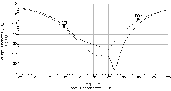
slotline, stripline, coplanar waveguide, and other topologies. Vias and airbridges connect topologies between layers, so as to simulate multilayer RF/microwave printed circuit boards, hybrids, multichip modules, and integrated circuits. Momen- tum gives a complete tool set to predict the performance of high-frequency circuit boards, antennas, and Ics. Momentum enables you to simulate when a circuit model range is exceed- ed or the model does not exist, so as to identify parasitic cou- pling between components. It enables to go beyond simple analysis and verification to design automation of circuit per- formance and Visualize current flow and 3-dimensional dis- plays of far-field radiation. Key features of Momentum in- clude Full integration in the ADS circuit simulation environ- ment allowing EM/Circuit co-simulation and co-optimization. Following simulation result indicate actual response taking parasitic coupling and stray magnetic field into consideration without isolation provided through ground plane. Figure 1 shows better performance of -33dB for EM simulation as compaired to schematic simulation.
Figure 1. Schematic and EM simulation for S11
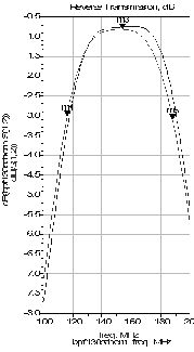
Figure 2 shows slight shift in frequency towards lower range for EM simulation as compaired to schematic simula- tion.
IJSER © 2013 http://www.ijser.org
International Journal of Scientific & Engineering Research, Volume 4, Issue 8, August-2013 990
ISSN 2229-5518
Figure 2. Schematic and EM simulation for S12
4.3 EM WITH ISOLATION AND METAL BOX
The EM simulation process uses the Green’s functions computed for the substrate, along with the mesh pattern to calculate the currents in the design. S-parameters are then computed based on the currents. For practical RF system, RF isolation and EM isolation are very important. So in this simu- lation level vias ground of 28 mil diameter at regular distance
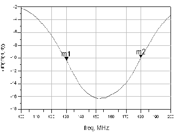
50 mil on PCB where implemented as part of RF isolation. And metal box of PCB dimension with 10 mm plate height from PCB is used for EM isolation. These elements enable you to specify boundaries on substrates along the horizontal plane. Without a box the substrate is treated as being infinitely long in the horizontal direction. This treatment is acceptable for many designs, but there may be instances where a boundaries need to be taken into account during the simulation process like patch antenna design.
Figure 3. EM Simulation with RF isolation and metal box. (m1 marker representes S11 = -10.77dB at 130MHz and m2
S11 =-10.03 dB at 180MHz)
A box specifies the boundaries as four perpendicular, verti- cal walls that make a box around the substrate. The walls of the box are perfect metal. Adding a box to the circuit enables you to analyze the effects of enclosing the circuit in metal, for example, to identify box resonance. Box resonance can have a significant effect on S-parameters in a small band centered around the box resonance frequency. When a simulation is performed, the resonance frequencies will be noted in the sta- tus window when the circuit is simulated; along with the fre- quency bands where no smooth S-parameters can be calculat- ed.following simulation result indicate improvement response characteristics with reduced adrupt responses due to proper RF isolation and EM metal box shielding.
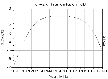
Figure 4. EM Simulation with RF isolation and metal box
5 HARDWARE RESULT
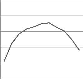
FR-4 dielectric material with dielectic constant 4.6 is used for PCB manufacture. All passive inductors and capictor used are SMT (Surface Mount Technology) component with desired Case size depending on PCB design. Figure below indicate the designed circuit in metal box for EM sheilding and output response as seen on spectrum analyzer at 150 MHz. Readings obtained from frequency spectrum are plotted in Fig.7.
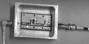
Figure 5. Designed Bandpass filter with metal box.
IJSER © 2013 http://www.ijser.org
International Journal of Scientific & Engineering Research, Volume 4, Issue 8, August-2013 991
ISSN 2229-5518
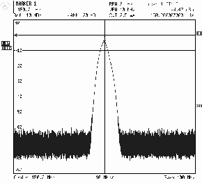
Figure 6. Output response on frequency spectrum.
Frequency (MHz)
0
Fig-
REFERENCES
[1] Randall W. Rhea, “HF FILTER DESIGN AND COMPUTER SIMULA- TION” , Noble Publishing
Atlanta .
[2] Robert C. Dixon,“ Radio Receiver Design”, Marcel Dejjer,Inc. 1998.
[3] A. A. Abidi, “Direct-conversion radio transceivers for digital com- munications,” IEEE Journal of Solid-State Circuits, 30, 12, 1399–1410, Dec. 1995.
[4] J. Crols and M. S. J. Steyaert, “Low-IF topologies for high- performance analog frontends of fully integrated receivers,” IEEE Transactions on Circuit and Systems—II: Analog and Digital Signal Pro- cessing, 45, 3, March 1998.
[5] B. Razavi, “Design considerations for direct-conversion receivers,”
IEEE Transactions on Circuit and Systems, 44, 6, 428–435, June 1997.
[6] G. Groenwold, “The design of high dynamic range continuous-time
integrable bandpass filters,” IEEE Transactions on Circuit and Systems,
38, 838–852, August 1991.
[7] J. O. Voorman, “Continuous-time analog integrated filters,” in Inte- grated Continuous- Time Filters, IEEE Press, New York, pp. 27–29.
1993.
[8] Devendra K. Misra, “ RADIO-FREQUENCY AND MICROWAVE COMMUNICATION ANALYSIS AND DESIGN”, John Wiley & Son, INC., 2004 .
[9] D.G. Swanson, J.R Hoefer , “Microwave Circuit Modeling Using Elec- tromagnetic Field Simulation” ,Artech House 2003.
[10] J. Laskar, B. Matinpour S. Chakraborty, “MODERN RECEIVER FRONT-ENDS Systems, Circuits, and Integration”, John Wiley &
100 120 140 160 180 200
Son, INC., 2004 .
-3
-6
-9
-12
-15
Figure 7. Filter response in bandwidth 100-200MHz
6 CONCLUSION
Complete design and anayasis of RF BPF filter for Radar is done capturing various functionality of Agilient’s ADS soft- ware. Performance enhancement of designed RF system due to metal shielding and RF isolation were observed. Simulation results of three cases of schematic, EM Momentum simulation, EM with RF isolation and metal box were analyized . Results indicate Substantial improvement in response characteristics, VSWR and interference isolation after inclusion of RF isolation and metal casing of circuit designed.
IJSER © 2013 http://www.ijser.org