The research paper published by IJSER journal is about Probe Storage 1
ISSN 2229-5518
Probe Storage
Sagar Ayare, Sandesh Pai
Abstract— Probe storage is a new technology of storage, which is a direct competitor to the existing HDD and Flash storage techniques. Probe storage is expected to use no more power than a flash memory card, but store up to 100 times as many bits as traditional disk storage. Future applications for parallel probes, including probe-based data storage and probe lithography, demand that probe technologies achieve patterning rates in the megahertz per probe range at feature sizes below 30 nm, i.e. ~1 Tbit in-2. In the paper which follows we first take an overview of the probe storage system and then describe it in detail. It is a fantastic technique of achieving densities as great as 641 Gb/sq in. (at present) which is more than four times the data density in a Flash-based devices. It uses a simple AFM (Atomic Force Microscope) tip to make indentations 10 nanometers in diameter in a plastic film. Each indentation is a bit, which can be heated back to its original shape. Driven by MEMS motors and all built into a chip, thousands of tiny probes, similar to the tips on an atomic force microscope, move back and forth a minute distance over the film. We also compare Probe storage with prominent data storage technologies and take a commercial perspective of it. Probe storage appears to be in a race, attempting to mature quickly enough at a given technology level that has not been surpassed by newer generations of the existing technologies by the time it is ready for production. It is not hard to realize that the feasibility and applications of Probe storage are wide and encompassing, and the cost will drop down dramatically once production starts in large volumes. This has been realized by large chip makers and tech giants such as Hitachi, Seagate, IBM, HP and many others. To say the least, Probe Storage is a promising technology that is here to stay and take data storage to new heights
Index Terms— Cantilevers, Microscanner , Positioning , Random Access, Scan Table, Storage Medium, Thermomechanical Sensor.
—————————— ——————————
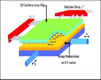
ROBE storage technology has been pioneered by Gerd Binnig and Peter Vettiger who developed the concept based on Atomic Force Microscopy activities. The basic concept uses a matrix of micro-machined cantilevers to write and read indentations in a polymer material. The cantilevers are bonded to a CMOS chip that holds an analogue sensing unit per cantilever and a multiplexer that transfers the data to
the main sensor and control component.
A magnetically actuated x/y scanner moves the storage media cantilevers relative to the cantilevers (see Figure 1). A mass-balanced design protects the media from shock in the x/y direction. In a single-lever test system the thermomechan- ical read/write mechanism has demonstrated a storage densi- ty of 641Gbit/in2 at raw bit-error rates of 10-4. Raw error rates of this order of magnitude are typical for magnetic recording. Standard error correction schemes can be used to get to the error rates required for today’s applications. The system archi- tecture, control and error correction codes are currently being developed MEMS components have been fabricated and as- sembled and are incorporated into a first small-scale prototype that serves as a test platform for the channel and control elec- tronics built on a dedicated printed circuit board. In parallel to the technical developments a commercial evaluation is performed to validate the competitiveness and market attractiveness of the technology against the most successful non-volatile memory technologies today: magnetic hard disc drive (HDD) and Flash.
————————————————
The attractiveness of a technology can only be analysed by looking at the attractiveness of derived products for particular applications and markets. In a commercial enterprise the busi- ness case will be analysed to evaluate the attractiveness of any investment in a new product. This analysis addresses the product, its cost and potential on the market but is driven by the strategic objectives of the organization and its capabilities such as the marketing and sales channels, the manufacturing expertise and capacity, and financial resources. Video and still picture cameras, and mobiles are the high volume applications in today’s consumer electronics. Flash cards and small HDDs are the two most important technologies that enable products for the applications
Sagar Ayare has pursued bachelor's degree in Electronics & Telecommuni- cations engineering from University of Mumbai, India, PH-+1-832-
4557722. E-mail: sagarayare87@gmail.com
Sandesh Pai has pursued bachelor's degree in Electronics & Telecommuni-
cations engineering from University of Mumbai ,India, PH-+91-
8861629896. E-mail: paisandesh@ymail.com Fig. 1. Probe Storage Concept Based on Array of Cantilever.
IJSER © 2012
The research paper published by IJSER journal is about Probe Storage 2
ISSN 2229-5518
Flash is a semiconductor device that follows the scaling rules of this technology. Increasing densities provide lower cost per storage bit. The cost per bit is however relatively high because of the overhead of a sensor per bit. A high demand and conse- quently high investments in Flash drive progresses the tech- nology and decreases cost.
Magnetic storage in HDD takes advantage of a single but expensive sensor that is addressing a magnetic disc and pro- vides low cost per bit. The unit costs are high because of the system overhead of the electronics and sensitive mechanics imposes a limit to the downscaling of the cost. In the next few years it is unlikely that another technology will compete with HDD in cost per GByte at high capacities, i.e. larger than
40GByte.However Flash products have the advantage of the best unit price for small and moderate storage capacity, i.e.
<10 GByte .
The emerging nano- and MEMS-based data-storage appli-
cation, which is called probe storage, has corporate researchers
in a feeding frenzy. Packing humongous memories in Lillipu-
tian packages, probe drives are prime candidates to combine the low cost, high capacity, and random-access features of
ordinary magnetic hard-disk drives with the low power draw, high data rate, small size, and nonvolatility of solid-state flash memories. Probe drives can cram a terabit (128 gigabytes) into each square inch of memory media. For contrast, conventional magnetic hard drives, such as the one-inch microdrives found in products like the Apple iPod, can at best achieve only 250 to
300 gigabits per square inch. The huge capacity of probe sys- tems translates into as many as 125 hours of DVD-quality vid- eo recording time.
Like a hard disk drive or an optical disc drive, a probe- drive system accesses data at random locations by reading current through the tips as they pass over the bits to determine whether they are 1s or 0s. Control circuitry aligns the mechan- ical components with nanometer precision, and error- correction codes ensure the integrity of the data being written and read.
The core components of this probe storage system are a two- dimensional array of silicon probes (cantilevers) and a micro- mechanical scanner which moves the storage medium relative to the array. A sophisticated design levels the probes above the storage medium with high precision and ensures that ex- ternal vibrations and impacts. For the device to perform its reading, writing and erasing functions, the cantilever tips are brought into contact with the storage medium — a thin film of a custom designed cross-linked polymer coated on a silicon substrate, which is moved in the x- and y-directions. The stor- age medium is positioned with nanometer-scale accuracy rela- tive to the cantilever array.
Most recent array design consists of an array of 64 × 64 canti- levers (4096) on a 100 µm pitch. The 6.4 × 6.4 mm² array is fab-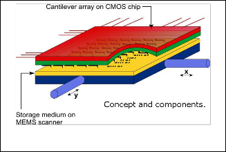
ricated on a 10 × 10 mm² silicon chip using a newly developed "transfer and join" technology that allows the direct intercon- nection of the cantilevers with CMOS electronics used to con- trol the operation of the cantilevers. With this technology the cantilevers and CMOS electronics are fabricated on two sepa- rate wafers.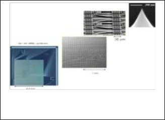
Fig. 2. Concepts & Components
Fig. 3. Optical micrograph of 64 × 64 cantilever array chip and SEM images of the center of the array, one cantilever and a tip apex.
The cantilevers used in the array are of a three-terminal de- sign, with separate heaters for reading and writing, and a ca- pacitive platform for electrostatic actuation of the cantilevers in the z-direction. The cantilevers are approximately 70 µm long, with a 500-700 nm long tip integrated directly above the write heater. The apex of each tip has a radius on the scale of a few nanometers allowing data to be written at extremely high densities (greater than 1 Tb/in²). In addition to the cantilevers, the array chip also carries eight thermal sensors which are used to provide x/y positioning information for closed-loop operation of the microscanner.
Movement of the storage medium relative to the cantilever array is achieved using a silicon-based x/y microscanner. The scanner consists of a 6.8 × 6.8 mm² scan table, which carries the polymer medium, and a pair of electromagnetic actuators. Both the scan table and the actuators are supported by silicon springs that are 10–12 µm wide and approximately 400 µm thick.
IJSER © 2012
The research paper published by IJSER journal is about Probe Storage 3
ISSN 2229-5518
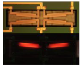
Fig. 4. Silicon Microscanner.
The scanner chip is mounted on a silicon base plate, which acts as the mechanical ground of the system and provides a clearance of approximately 20 µm between its top surface and the bottom surface of the moving parts of the scanner. The scan table can be displaced approximately 120 µm in two or- thogonal directions (x and y) using the two electromagnetic actuators. Each actuator consists of a pair of permanent mag- nets mounted in a silicon frame, with a miniature coil mount- ed between them on the base plate. The actuator motion is coupled to the scan table using a pivot and a mass-balancing scheme, which makes the system robust against external vi- brations and shock.
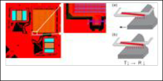
Positioning information for the closed-loop operation of the scanner is provided by two pairs of thermal position sensors. These sensors are fabricated on the cantilever-array chip and positioned directly above the scan table. The sensors consist of thermally isolated, resistive strip heaters made of moderately doped silicon. Each sensor is positioned above an edge of the scan table and heated by applying a current. A fraction of this heat is conducted through the ambient air into the scan table, which acts as a heat sink. Displacement of the scan table gives rise to a change in the efficiency of this cooling mechanism, resulting in a change in the temperature of the heater and thus a change in its electrical resistance. These sensors provide an effectively linear position signal over the entire 120 µm range of the scanner, with a resolution of less than 2 nm in a 10 kHz bandwidth
Fig. 5. Schematic of position- sensing concept.
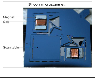
Fig. 6. Optical micrograph of position sensors.
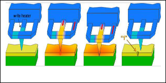
Thermo-mechanical writing is performed by locally softening the polymer medium using the heated tip of a cantilever and simultaneously applying a force to create a nano-scale inden- tation in the polymer film. The tip is heated by applying a cur- rent pulse to a resistive heater integrated into the cantilever, directly behind the tip. During writing, the tip is heated to a temperature above the glass transition temperature of the pol- ymer and forces on the order of a few hundred nanonewtons are applied to the tip for a few microseconds
Fig. 7. Thermomechanical writing.
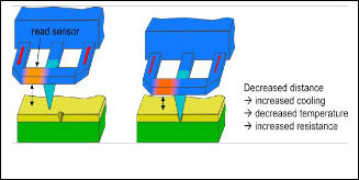
Read-back of the data is performed using a thermo-mechanical sensing technique in which a second resistive heater integrat- ed into the cantilever is heated to a temperature of around 200
°C while the polymer medium is scanned under the tip. The
principle of thermal sensing is based on the fact that the rate of
cooling of this heater increases as the distance between it and
the substrate carrying the polymer medium is reduced. Thus,
when the tip moves into an indentation, the distance between
the heater and substrate is reduced, resulting in an increase in cooling and hence a decrease in the temperature of the heater.
This change in temperature results in an increase in resistance of the heater, which is easily detected by monitoring the cur- rent flowing through it
IJSER © 2012
The research paper published by IJSER journal is about Probe Storage 4
ISSN 2229-5518
Fig. 8. Thermomechanical reading.
In the thermal-mechanical writing process described above, indentations are created by elastically straining the locally softened polymer by applying a force. This stress is then fro- zen into the film by rapidly cooling the material, resulting in the creation of a "meta-stable" indentation. If the polymer is reheated, the polymer softens, thereby allowing the stored elastic strain to relax, and hence erasing the indentation. This can be done at the individual bit level by using the tip as a localized heat source. For example, writing a new indention very close to a previous one results in the erasure of the old indentation and the creation of a new one. Hence, a previously written data track can be erased simply by overwriting it with a series of closely spaced indentations. In other words, erasing is essentially similar to writing at a narrower pitch between indentations.
Ongoing research on the write, read and erase operations concentrates on reducing the energy required to form an in- dentation, on the effects of repeated erasing and re-writing on tip and medium wear and on extending the lifetime of written indentations.
The device also includes thermal position sensors that provide x/y-position information to the servo controller. MEMS-based storage devices require a closed-loop servo system to write uniformly spaced data tracks and to read them back with suf- ficient accuracy to ensure a low error rate. As the areal density of such a system is being increased to the Tb/in² regime and beyond, the performance requirements for the servo system become severe. In general, the servo system in such a storage device has two functions. First, to locate the target track to which information is to be written or read from, starting from an arbitrary initial position of the scan table carrying the stor- age medium.
In prototype MEMS-based storage device, the thermal position sensors provide x/y-position information to the servo controller during the seek/settle mode of operation. The se- cond function of the servo system is to maintain the position of the read/write probes on the center of the target track as they are being scanned along the length of this track during normal read/write operation. This is achieved by the track- follow procedure, which controls the fine positioning of the read/write probes in the cross-track direction and is critical for reliable storage and retrieval of user data.
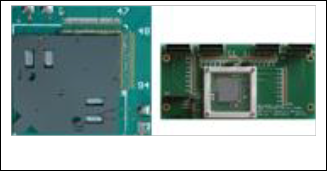
The probe storage system prototype that has been developed consists of the following components: · a MEMS part in form factor, comprising: - a 2-D array of 32 cantilevers for data, servo and timing purposes; - a microscanner; - 2 pairs of thermal positioning sensors, one pair for each direction of mo- tion; · analog front-end electronics, implemented in discrete components, for parallel operation of up to 8 levers; · a read channel, comprising the data and servo detector and the servo controller, all implemented in an on-board DSP; · a system controller, comprising the modulation encoder/decoder and the ECC encoder/decoder, implemented in an FPGA on board; · a host interface, according to the Compact Flash standard. Using this small-scale prototype, scientists have demonstrated the storage and retrieval of user data using mul- tiple levers at densities up to 517 Gb/in².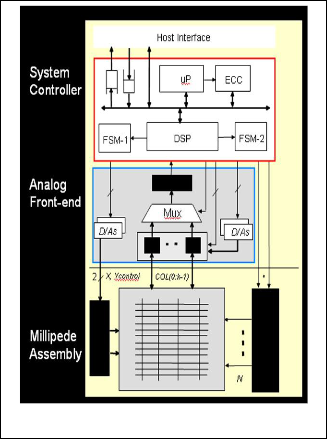
Fig. 9. Prototype Board acquisition circuitry
Fig. 10. System Architecture
IJSER © 2012
The research paper published by IJSER journal is about Probe Storage 5
ISSN 2229-5518
Probe storage systems can be used for micro drives, which will feature very small form factor, enabling use in small footprint devices like watches, mobile phones and personal media sys- tems, and at the same time provide high capacity. The very high data density of millipede systems makes them a very good candidate to be put to this use.
The Millipede system provides high data density, low seek times, low power consumption and, probably, high reliability. These features make them candidates for building high capaci- ty hard drives, with storage capacity in the range of terabytes. Although the data density of a Probe device is high, the capac- ity of an individual device is expected to be relatively low -- on the order of single gigabytes. Thus replacing hard drives probably requires economically collecting around 100 minia- ture devices into a single enclosure.
The mobile storage market is attractive because of the high growth of mobile devices that are demanding ever increasing storage capacity. In mobile applications the environmental stress on a device is an important challenge. The most im- portant factors are an operating temperature over a wide range (e.g. -20°C to 85°C) and shock resistance (e.g. 1 m drop of a host device on concrete). A permanent loss of data is not acceptable. Semiconductor storage has distinct advantages for these requirements.
Probe Storage is a technology that enables storing huge amounts of data in a small size at a great speed while consum- ing less power. Hence, it is likely to be used as the most suited storage medium in Micro Hard Drive based devices.
[1] P. Vettiger, G. Cross, M. Despont, U. Drechsler, U. Du¨ rig, B. Gotsmann, W. Ha¨ berle, et al., ‘‘The ‘Millipede’— Nanotechnology Entering Data Storage,’’ IEEE Trans. Nanotechnol. 1, No. 1, 39–55 (2002)
[2] G. Binnig, C. F. Quate, and Ch. Gerber, ‘‘Atomic Force Microscope,’’ Phys. Rev. Lett. 56, No. 9, 930–933 (1986). Journal of Magnetism & Magnetic Materials
[3] Nanochip magazine
[4] www.pcmag.com
[5] www.hp.com
IJSER © 2012