International Journal of Scientific & Engineering Research, Volume 4, Issue 6, June-2013 1700
ISSN 2229-5518
Power and Area Efficient Design of
Reconfigurable Crossbar Switch for BiNoC Router
Mr. Ashish Khodwe, Mrs. V. K. Rajput, Prof.C.N.Bhoyar, Prof. Priya M. Nerkar
Abstract—Network-on-Chip (NOC) has been proposed as an attractive alternative to traditional dedicated wire to achieve high performance and modularity. Power and Area efficiency is the most important concern in NOC design. Small optimizations in NoC router architecture can show a significant improvement in the overall performance of NoC based systems. Power consumption, area overhead and the entire NoC performance is influenced by the router crossbar switch. This paper presents implementation of 10x10 reconfigurable crossbar switch (RCS) architecture for Dynamic Self-Reconfigurable BiNoC Architecture for Network On Chip. Its main purpose is to increase the performance, flexibility. W e implemented a parameterized register transfer level design of reconfigurable crossbar switch (RCS) architecture. The design is parameterized on (i) size of packets, (ii) length and width of physical links, (iii) number, and depth of arbiters, and (iv) switching technique. The paper discusses in detail the architecture and characterization of the various reconfigurable crossbar switch (RCS) architecture components. The characterized values were integrated into the VHDL based RTL design to build the cycle accurate performance model. In this paper we show the result of simple 4 x4 as well as 10x10 crossbar switch .The results include VHDL simulation of RCS on ModelSim tool for 4 x4 crossbar switch and Xilinx ISE 13.1 software tool for 10x10 crossbar switch.
Index Terms— Interconnection networks, on-chip communication, Reconfigurable, crossbar switch .networks-on-chip (NoCs)
1. INTRODUCTION
Modern Systems contain multiple processors, dedicated hardware processing units and peripherals. As technology advances with ever increasing processor speed, global wires spanning across significant portion of board size will dominate the propagation delay [1], which becomes a performance bottleneck for systems design. In recent years, significant research has demonstrated that an on- chip packet interconnection network is a better candidate for handling on chip communication [2]. System modules communicate to one another by sending packets across the network. This approach has the advantages of both performance and modularity. In another example [3], researchers implemented such a reconfigurable interconnection network on FPGA for improved hardware-software multitasking. The system level components include, besides the on-chip network, also embedded software. Some communication networks that target general-purpose multi processors are the J-Machine [4] and Smart Memory [5]. However, very little research has been done on modeling the on-chip communication architecture and integrating the communication network with processor units in a single environment.
As the industry builds multi-core architecture involving
————————————————
Mr. Ashish Khodwe, Department of Electronics Priyadarshini college of
Engineering ,RTMNU,Nagpur,India.(khodweashish@gmail.com)
Mrs. V. K. Rajput, Department of Electronics Priyadarshini college of
Engineering ,RTMNU,Nagpur,India.( vasanti.rajput1@gmail.com ) Prof.C.N.Bhoyar, Department of Electronic Priyadarshini College of Engineering, RTMNU, Nagpur, India (cnbhoyar@yahoo.com)
Prof. Priya M. Nerkar, Department of Electronics Priyadarshini college of
Engineering ,RTMNU,Nagpur,India.( priyanerkar@yahoo.in)
tens and hundreds of cores in the future, on-chip interconnection networks have emerged as a promising candidate for solving the wire-delay problem facing current chip multiprocessors (CMPs) [6], [2]. However, one of the major research challenges currently faced by on-chip interconnection network designers is that of power dissipation [12]. NoC architectures are characterized by the links for data transmission and the routers for storing, arbitration and switching functions performed by input buffers, arbiters and the crossbar respectively. Power is dissipated both for communicating data across links as well as for switching and storage within the routers [12]. With the increasing need for low power architectures, NoC research has focused on optimizing buffer design [9], [10], [11], minimizing crossbar power [8], [12], and utilizing 3D interconnects [13]. Modular router design ensures that the network bandwidth and storage is shared evenly among all the input channels and packets. This effective sharing of resources (buffer and channel) is achieved by implementing routing, crossbar switch and switch allocation functionalities within the router on a hop-by- hop basis. Additionally, broadcasting of communication information across every node adds power (0.6 mW/TX and 0.4 mW/RX). Reducing the size of the input router crossbar switch is a natural approach to reduce the power to read/write a flit and area overhead of the router. However, the network performance and flow control is primarily characterized by the input buffers [15].
However, at high loads, blocking probability increases
due to wire-to-wire transfers. Therefore, we design a
larger crossbar 10 × 10 to provide bypass path at all loads.
Although a larger crossbar occupies more area, recent work on high-radix routers show that these designs are feasible for on-chip networks [16]. Moreover, double-
IJSER © 2013 http://www.ijser.org
International Journal of Scientific & Engineering Research, Volume 4, Issue 6, June-2013 1701
ISSN 2229-5518
pumped crossbar designed for Intel Teraflops which reduces the size of the crossbar by 57% could be adopted for our design. In this context, applying concepts from computer and telecom networks to embedded systems, a new interconnection structure, named Network on Chip (NoC) is emerging [16][17][18]. NoCs [11] can replace busses due to the following features: (i) energy efficiency and reliability [16]; (ii) scalability of bandwidth when compared to traditional bus architectures; (iii) reusability; (iv) distributed routing decisions [17][18].
Our application presented here is the first step towards
the implementation of the different components of a
BiNoC router. The goal of this work is to describe the
implementation and evaluation of reconfigurable crossbar
switch in BiNoCs router. Implementation of routers with reconfigurable crossbar switch is complex due to the degree of freedom to choose schemes for buffering, internal interconnections, arbitration and routing. Silicon area constrains the complexity of these schemes. Primary function is communication, and not processing. The evaluation of Area and power of BiNoCs with reconfigurable crossbar switch enables designers to parameterize the network according to application requirements. This paper is organized as follows. Section
2 given related work, section 3 presents an overview of the state of the art in BiNoCs using reconfigurable crossbar switch. Section 4 details the main contribution of this work, the implementation of reconfigurable crossbar switch in the BiNoC router. Section 5 shows experimental result for reconfigurable crossbar switch.
2. RELATED WORK
With the invention of the telegraph in 1836 and the telephone in 1876 a need arose for central switches to connect the expanding number of devices. The first switches were large boards with human operators physically wiring connections. In 1888 A. B. Stroweger created an automated electro-mechanical switch [21]. To make a connection, a mechanical arm rotated in a plane, selecting 1 of 10 contacts. A Two-Motion Selector extended the idea by enabling the switch to first select from 10 planes, enabling 100 connections. In the early
1900’s G. A. Betulander, a Swedish engineer, developed and produced a crossbar switch that used electro- mechanical relays to make connections in a single plane [22]. After the advent of transistors, Bell Labs introduced the 1ESS in 1965, the first computerized central office telephone switch [23]. It featured a central memory and stored program control. However, signal transmission was still analog. By the early 1970’s digitally controlled digital transmission switches began appearing [24]. With the advent of FPGAs in 1984, run-time reconfigurable circuits became possible. Algotronix created partially configurable FPGAs. Platforms for configurable
computing were introduced [25]. Toolkits enabling reconfiguration were created [26, 27]. Applications utilizing reconfiguration, like neural nets [28], DES [29]and AES cryptography [30], bioinformatics [31], signal processing [32], and CAMS [33, 34] became available. There are lots of commercial network processors of different companies. Some companies and respective network processors [36] are: IBM (NP4GS3), Motorola/CPort (C-5 Family), Lucent/Agere (FPP/RSP/ASI), Sitera/Vitesse (IQ2000), Chameleon (CS2000), EZChip (NP- 1), Intel (IXP1200) and others. None of them presents reconfigurability, except the CS2000 of Chameleon [22]. However, it does not have a reconfigurable crossbar switch. There are some documents and papers about crossbar switch, but nothing using reconfigurable crossbar in a network processor. The related works [20] [21] [35] present results of implemented crossbar switch on FPGA. The Flexbar [28] work proposes to modify the scheduler and network hardware levels, but the crossbar architecture core is similar to a traditional crossbar switch (TCS). The paper does not relate FPGA and the reconfigurable computing [22] as a feature of Flexbar.

Fig.1 R2NP (Reconfigurable RISC Network Processor) architecture
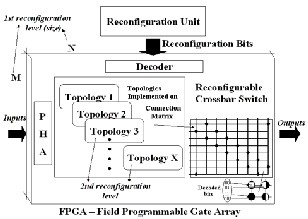
The figure 1 presents the R2NP (Reconfigurable RISC Network Processor) architecture [22]. The R2NP has been used as a base for the design of the reconfigurable crossbar switch architecture. Thus, the design of RCS (Reconfigurable Crossbar Switch) was based on the use of it in a network processor. RCS, presented in figure, has three main blocks: (1) connection matrix, where the topologies are implemented ;(2)decoder, that converts the reconfigurable bits for a matrix bits set and (3) pre-header analyzer (PHA). NPs can add a pre-header in the packet with the output destination. Reconfigurable crossbar switch (RCS) uses reconfiguration bits to implement the topology in the space. The reconfiguration bits set are capable of reconfiguring or implement a new topology in
IJSER © 2013 http://www.ijser.org
International Journal of Scientific & Engineering Research, Volume 4, Issue 6, June-2013 1702
ISSN 2229-5518
RCS whenever necessary. These nodes determine which connections will be closed and consequently which paths exist through the crossbar switch. RCS has two bits of reconfiguration to each node, which define the current topology. Only the Reconfiguration Unit and the instruction set of the network processor are able to change those bits in order to implement new topologies. Although one instruction can modify a reconfigurable bit, it only modifies the 01 and 10 formats the 00 and 11 formats are restricted to Reconfiguration Unit.
3. BINOC ARCHITECHURE

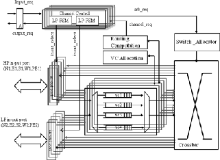
Fig.2 Modified four-stage pipelined router architecture for our proposed BiNoC router with VC flow-control technique.
Fig.2 shows the microarchitecture of A bidirectional channel network-on-chip (BiNoC) router is modeled [38]. This section to enhance the performance of on-chip communication. In a BiNoC, each communication channel allows itself to be dynamically reconfigured to transmit flits in either direction. This added flexibility promises better bandwidth utilization, lower packet delivery latency, and higher packet consumption rate. Novel on- chip router architecture is developed to support dynamic self-reconfiguration of the bidirectional traffic flow. The flow direction at each channel is controlled by (CDC) a channel-direction-control protocol [38]. Implemented with a pair of finite state machines. This channel-direction- control protocol is shown to be of high performance, free of deadlock, and free of starvation.
Fig.2 illustrates reconfigurable crossbar switch
components of a BiNoC router.
3.1 Crossbar Traversal
Flits that have been granted passage on the crossbar are passed to the appropriate output channel. The following sections describe in more detail each of the router’s components.
3.2 Switch Allocation
Individual flits arbitrate for access to physical channels via the crossbar on each cycle. Arbitration may be performed in two stages [5]. The first reflects the sharing of a single crossbar port by V input virtual-channels; this requires a V-input arbiter for each input port. The second stage must arbitrate between winning requests from each input port (P inputs) for each output channel. The scheme is illustrated in Figure 3. The request for a particular output port is routed from the VC which wins the first stage of arbitration. In order to improve fairness, the state of the V-input the second stage of arbitration. We assume this organization wherever multiple stages of arbitration are present. This switch allocator organization may reduce the number of requests for different output ports in the first stage of arbitration, resulting in some wasted switch bandwidth.

Fig. 3 SA in a BiNoC router
3.3 Arbiter
Arbiter controls the arbitration of the ports and resolves contention problem. It keeps the updated status of all the ports and knows which ports are free and which ports are communicating with each other. Packets with the same priority and destined for the same output port are scheduled with a round-robin arbiter. Supposing in a given period of time, there was many input ports request the same output or resource, the arbiter is in charge of processing the priorities among many different request inputs. The arbiter will release the output port which is connected to the crossbar once the last packet has finished transmission. So that other waiting packets could use the output by the arbitration of arbiter.
IJSER © 2013 http://www.ijser.org
International Journal of Scientific & Engineering Research, Volume 4, Issue 6, June-2013 1703
ISSN 2229-5518

Fig.4 Arbiters in a Crossbar Switch Module
3.4 Crossbar
A crossbar switch (also known as cross-point switch, cross point switch, or matrix switch) is a switch connecting multiple inputs to multiple outputs in a matrix manner. The design of crossbar switch has 10 inputs and 10 outputs. In the architecture illustrated in Figure 2 each input port is forced to share a single crossbar port even when multiple flits could be sent from different virtual- channel buffers. This restriction allows the crossbar size to be kept small and independent of the number of virtual- channels. Dally [36] and Chien [37] suggest that providing a single crossbar input for each physical input port will have little impact on performance as the data rate out of each input port is limited by its input bandwidth.
4. RECONFIGURABLE CROSSBAR SWITCH

Fig.5 FPGA –Reconfigurable Crossbar Switch
Two approaches to dynamic reconfiguration of NoC
1. Adding reconfiguration logic which incurs area
overhead 2. Partial reconfiguration (PR).
The reconfigurable crossbar switch fig.5 has some
connection nodes, which, if closed, compose a circuit. This
circuit represents a topology in space. Differently from a
traditional crossbar switch (TCS), where it is possible to
close only one node per line or column, regards the
implemented topology, the (RCS) permits that more than one node can be closed per line or column at the same time. The reconfigurable crossbar switch (RCS) uses reconfiguration bits to implement the topology in the space. That topology actually maintains the created connections as a circuit. The reconfiguration bits set are capable of reconfiguring or implement a new topology in (RCS) whenever necessary.
5. EXPERIMENTAL RESULTS
5.1 Performance Evaluation
In this section, we present simulation-based performance evaluation of our architecture, BiNoC router with reconfigurable crossbar switch technique in terms of network latency, energy consumption .We describe our experimental methodology, and detail the procedure followed in the evaluation of these architectures.
5.2 Simulation setup
In this section the synthesis results will be presented, and a cost analysis of area and power consumption will be made based on the synthesis results. The proposed BiNoC routers with reconfigurable crossbar switch technique were implemented in structural Register- Transfer Level (RTL) VHDL. A Router with parametrable flit size and 4 flits buffer depth and five ports have been modeled with VHDL language on RTL level. They were simulated and synthesized respectively by using the ISE 13.1 tool.
5.3 Reconfigurable Crossbar Switch Validation

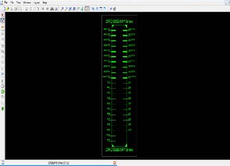
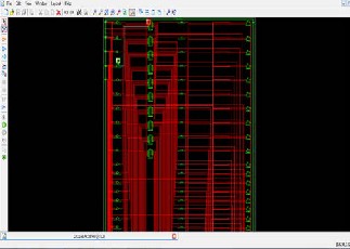
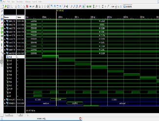
The Crossbar Switch channel was described in VHDL and validated by functional simulation. Fig.6 shows functional simulation result of reconfigurable crossbar switch in BiNoC router. This simulation is performed on Active- HDL software.
IJSER © 2013 http://www.ijser.org
International Journal of Scientific & Engineering Research, Volume 4, Issue 6, June-2013 1704
ISSN 2229-5518

Fig.6 RTL simulation view of Reconfigurable Crossbar Switch


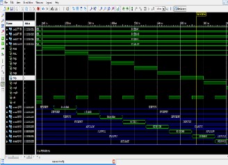
Fig.7 Reconfigurable 10x10 Crossbar switch Xilinx ISE 13.1 software tool waveform simulation.

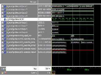
Fig.8 Reconfigurable 4x4 Crossbar switch ModelSim software tool waveform simulation

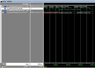
Fig.9 Pre-header analyzer (PHA) waveform simulation.

Fig.10: Power breakdown for 10x10 Reconfigurable Crossbar Switch
(RCS)
IJSER © 2013 http://www.ijser.org
International Journal of Scientific & Engineering Research, Volume 4, Issue 6, June-2013 1705
ISSN 2229-5518
5.4 Power breakdown
The total dynamic power consume for a 128-bit flit in the buffer is estimated to be 2.8 mW shown in fig.9
5.5 Area breakdown
The architecture was prototyped on a Spartan 3A FPGA, the hardware occupancy of the system in terms of FPGA slices has been provided in table I.
Table I. Area breakdown result of Reconfigurable Crossbar
Switch (RCS) BiNoC router architecture
Resources | Mapping to Spartan 3A FPGA Device |
Resources | Used | Available | Utility % |
Resources | RCS | Available | RCS |
Slices | 274 | 1792 | 15% |
Slices+ FF | 56 | 3584 | 1% |
4 input LUT | 512 | 3584 | 14% |
Bonded IOBs | 182 | 195 | 93% |
5.6 Area Measurement
BiNoC router architectures in terms of logic gate count and percentage calculated by synopsys design compiler [40].
Area and Power breakdown of BiNoC_4VC
Table I shows Area breakdown of BiNoC_4VC [38]
Component buff. Depth | BiNoC_4VC(16) 4 flits x 4 |
Component buff. Depth | Area (gate count) | Power (mW) |
Input buf. + buf. ctrl | 18,722 | 16.90 |
Routing computation | 669 | 0.48 |
VC allocation | 12,295 | 5.76 |
Switch allocation | 2,245 | 1.75 |
Switch traversal | 4,402 | 2.35 |
Bidir. ch. ctrl | 1,628 | 0.68 |
Total | 39,960 | 27.94 |
6. ACKNOWLEDGEMENTS
Authors wish to remark the great task carried out by the Xilinx and Modelsim user guide; and the authors wish to thank Prof. C.N.Bhoyar and Prof. Priya M. Nerkar for his contribution in the design process.
7. CONCLUSION
We have represented an innovative Reconfigurable Crossbar Switch for BiNoC architecture and demonstrated its performance enhancement With Reconfigurable Crossbar Switch, we anticipate that Reconfiguration has the potential of supporting better congestion control schemes, differentiated services and fault tolerance capability to accommodate more diverse services in the future. The contribution of this paper is the proposed RCS architecture. The first level of reconfiguration of the RCS could be reached through the codification of the architecture using a hardware description language, allowing it to be implemented in several devices with dimensions determined by device capacity. The second level of reconfiguration could be reached with modifications in the matrix of connections. These modifications generate an overhead. However, through the experiments, it was evidenced that the overhead time is less than the speedup obtained through the topologies implementation in RCS. Therefore, the RCS- has a better performance when compared to a TCS.
REFERENCES
[1] S. Charles,”Let’s Route Packets Instead of Wires,” Proc. 6th
MIT Conf. 1990, Advance Research in VLSI, pp. 133-138.
[2] L. Benini and G. Micheli, “Networks on Chips: A New SoC Paradigm,” IEEE Computer 35(1) 2002, pp. 70-78.
[3] T. Marescaux, A.Bartic, D.Verkest, S.Vernalde, R. Lauwereins, “Interconnection Networks Enable Fine-Grain Dynamic Multi- Tasking on FPGAs,” FPL, Sep, 2002.
[4] W.Dally, “The J-Machine Network” Proc Intnl Conf on
Computer Design. IEEE VLSI in Computer & Processor, Oct
1992, pp 420-423.
[5] K. Mai,” Smart Memories: A Modular Reconfigurable
Architecture,” Proc ISCA, June 2000, pp. 161-71.
[6] W. J. Dally and B. Towles, “Route packets, not wires,”in Proceedings of the Design Automation Conference(DAC), Las Vegas, NV, USA, June 18-22 2001.
[7] J. D. Owens, W. J. Dally, R. Ho, D. N. Jayasimha, S.W. Keckler, and L. S. Peh, “Research challenges foron-chip interconnection networks,” IEEE Micro, vol.27, no. 5, pp. 96–108, September- October 2007.
[8] Y. Hoskote, S. Vangal, A. Singh, N. Borkar, and S.Borkar, “A 5- ghz mesh interconnect for a teraflopsprocessor,” IEEE Micro, pp. 51–61, Sept/Oct 2007.
[9] J. Hu and R. Marculescu, “Application-specific bufferspace allocation for network-on-chip router design,” inProceedings of the IEEE/ACM InternationalConference on Computer Aided Design (ICCAD), SanJose, CA, USA, November 7-11 2004, pp.
354–361.
[10] C. A. Nicopoulos, D. Park, J. Kim, N. Vijaykrishnan,M. S.
Yousif, and C. R. Das, “Vichar: A dynamicvirtual channel
regulator for network-on-chip routers,”in Proceedings of the
39th Annual InternationalSymposium on Microarchitecture
(MICRO), Orlando,FL, USA, December 9-13 2006, pp. 333–344.
[11] A. K. Kodi, A. Sarathy, and A. Louri, “ideal: Interroutedual- function energy and area-efficient links fornetwork-on-chip (noc) architectures,” in Proceedings ofthe International Symposium on Computer Architecture(ISCA), June 2008, pp.
241–250.
IJSER © 2013 http://www.ijser.org
International Journal of Scientific & Engineering Research, Volume 4, Issue 6, June-2013 1706
ISSN 2229-5518
[12] H. S. Wang, L. S. Peh, and S. Malik, “Power-drivendesign of router microarchitectures in on-chipnetworks,” in Proceedings of the 36th AnnualACM/IEEE International Symposium onMicroarchitecture, Washington DC, USA, December03-05
2003, pp. 105–116.
[13] S. E. Dongkook Park, R. Das, A. K. Mishra, Y. Xie, N.Vijaykrishnan, and C. R. Das, “Mira: A multi-layeredon-chip interconnect for router architecture,” inProceedings of the International Symposium onComputer Architecture (ISCA), June 2008, pp. 251–261.
[14] W. J. Dally and B. Towles, Principles and Practices of Interconnection Networks. San Fransisco, USA: Morgan Kaufmann, 2004.
[15] J. Kim, W. Dally, B. Towles, and A. Gupta “Microarchitecture of a high-radix router,” inProceedings of the 32th Annual International Symposium on Computer Architecture (ISCA’05), June2005, pp. 420–431.
[16] Kumar, S.; Jantsch, A.; Soininen, J. P.; Fonsell, M. “A Networkon Chip Architecture and Design Methodology”. In:Computer Society Annual Symposium on VLSI, 2002.
[17] Benini, L.; De Micheli, G. “Powering networks onchips: energy- efficient and reliable interconnect design forSoCs”. In: 14th International Symposium on Systems Synthesis,2001, pp. 33-38.
[18] Guerrier. P.; Greiner. A. “A generic architecture for on-chip packet-switched interconnections”. In: Design Automation and Test in Europe (DATE’00), 2000, pp. 250-256.
[19] D. E. Comer, “Network Systems Design using Network
Processors”, Prentice Hall, 2003
[20] D. Kim, K. Lee, S. Lee and H. Yoo, “A Reconfigurable Crossbar
Switch with Adaptive Bandwidth Control for
Networks-on-Chip”, IEEE International Symposium on Circuits and Systems, 2005, pp. 2369 - 2372
[21] S. Young, et al., “A High I/O Reconfigurable Crossbar Switch”,
11th Annual IEEE Symposium on Field- Programmable Custom
Computing Machines, Napa, Califormia, April 09-13, 2003,
pp.3-10.
[22] H. C. Freitas and C. A. P. S. Martins, “Didactic Architectures and Simulator for Network Processor Learning”, Workshop on Computer Architecture Education, San Diego, CA, USA, 2003, pp.86-95
[23] T. Farley. TelecomWriting.com’s Telephone History Series. 2001.
[24] L.E.S. Ramos and C.A.P.S. Martins, “A Proposal of Reconfigurable MPI Collective Communication Functions”. Third International Symposium on Parallel and Distributed Processing and Applications, LNCS 3758, Nanjing, China, November 2-5, 2005, pp. 102-107
[25] D. A. Buell, J. M. Arnold, and W. J. Kleinfelder. Splash 2: FPGAs in Custom Computing Machine. IEEE Computer Society Press, Napa Valley, Ca, 1996.
[26] P. Bellows and B. Hutchings. JHDL: An hdl for reconfigurable systems. In IEEE Symposium on FPGAs for Custom Computing Machines, pages 175–184, Napa Valley, Ca, April 1998. IEEE Computer Society.
[27] [ 9] S. A. Guccione and D. Levi. XBI: A java-based interface to FPGA hardware. In J. Schewel, editor, Configurable Computing: Technology and Applications, Proc. SPIE 3526, pages 97–102, Bellingham, WA, November 1998. SPIE – The International Society for Optical Engineering.
[28] J. Chang, S. Ravi, and A. Raghunathan, “FLEXBAR: A crossbar switching fabric with improved performance and utilization”, IEEECustom Integrated Circuits Conference, May 2002, pp.405-408
[29] C. Patterson. High performance des encryption in virtex fpgas using jbits. In K. L. Pocek and J. Arnold, editors, IEEE Symposium on FPGAs for Custom Computing Machines, Napa Valley, Ca, April 2000. IEEE Computer Society.
[30] [12] S. P. McMillan and S. A. Guccione. Partial run-time reconfiguration using JRTR. In R. W. Hartenstein and H. Grunbacher, editors, Field-Programmable Logic and Applications, pages 352–360, Berlin, August 2000. Springer-Verlag.
[31] E. Lemoine and D. Merceron. Run time reconfiguration of FPGA for scanning genomic databases. In K. L. Pocek and J. Arnold, editors, IEEE Symposium on FPGAs for Custom Computing Machines, pages 90–98, Napa Valley, Ca, April 1995. IEEE Computer Society.
[32] J. Scalera and M. Jones. A run-time reconfigurable plug-in for the winamp mp3 player. In K. L. Pocek and J. Arnold, editors, IEEE Symposium on FPGAs for Custom Computing Machines, pages 319–320, Napa Valley, Ca, April 2000. IEEE Computer Society.
[33] J. M. Ditmar. A dynamically reconfigurable FPGA-based content addressable memory for IP characterization. Master’s thesis, KTH-Royal Institute of Technology, Stockholm, Sweden,
2000.
[34] S. A. Guccione, D. Levi, and D. Downs. A reconfigurable content addressable memory. In J. R. et al., editor, Proceedings of the 15th International Parallel and Distributed Processing Workshops, pages 882–889, Berlin, May 2000. Springer-Verlag.
[35] H. Eggers, P. Lysaght, H. Dick, and G. McGregor, “Fast
Reconfigurable Crossbar Switching in FPGAs”, Proceedings of
6th International Workshop on Field-Programmable Logic and
Applications, Springer LNCS 1142, 1996, pp.297-306
[36] W. J. Dally, "Virtual-channel flow control," in Proceedings of the
17th Annual International Symposium on Computer
Architecture (ISCA), pp. 60-68, 1990.
[37] A. A. Chien. A cost and speed model for k-ary n-cube wormhole routers. In Proceedings of Hot Interconnects, 1993.
[38] Ying-Cherng Lan, Hsiao-An Lin, Shih-Hsin Lo, Yu Hen Hu, and Sao-Jie Chen, “A bidirectional noc (binoc) architecture with dynamic selfreconfigurable channel,” Computer-Aided Design of Integrated Circuits and Systems, IEEE Transactions on, vol.
30, no. 3, pp. 427 –440, march 2011.
IJSER © 2013 http://www.ijser.org

