
International Journal of Scientific & Engineering Research, Volume 6, Issue 3, March-2015 542
ISSN 2229-5518
PV Fed Modified SEPIC Converter
B.V.N.V.Shiv Kanth, C.V.S.Sainath, G.Sandeep
Tracking (MPPT), Modified SEPIC Converter , Photo Voltatic (PV) Cell ,Modified SEPIC Converter.
—————————— ——————————
One of the major concerns in the power sector is the day- to-day growing power demand but the absence of enough resources to meet the power demand using the conventional energy sources. Demand has enlarged for renewable sources of energy to be employed along with conventional systems to meet the energy demand. Renewable sources such as solar energy and wind energy are the foremost energy sources which are being employed in this regard.
Solar energy is plentifully available that has made it
possible to harvest it and utilize it correctly. Solar energy
can be a standalone generating unit or can be a grid connected generating unit depending on the obtainability of a grid nearby. Thus it is used to power rural areas where the obtainability of grids is very low.
In order to challenge the present energy disaster one has
to develop a capable manner in which power has to be extracted from the incoming solar radiation. The conversion mechanisms on power have been greatly reduced in size in the earlier few years [1]-[2]. The expansion in power electronics and material science has helped engineers to come up very small but powerful systems to withstand the high power demand. But the drawback of these systems is the enlarged power density. Development has set in for the use of multi-input converter units [3] that can successfully handle the voltage fluctuations. But due to great production cost and the low efficiency of these systems they can hardly participate in the competitive markets as a key power generation source.
The constant growth in the enlargement of the solar cells
manufacturing technology would absolutely make the use
of these technologies possible on a wider basis [4]-[8]. The use of the latest power control mechanisms called the Maximum Power Point Tracking (MPPT) algorithms has led to the progress in the efficiency of operation of the solar
modules and thus is active in the field of consumption of renewable sources of energy.

Fig. 1. PV cell modeled as diode circuit.
A photovoltaic system is a system which practices one or more solar panels to transform solar energy into electricity. It consists of various components, comprising the photovoltaic modules, electrical and mechanical connections and mounting.
PV cells are finished of semiconductor materials, like silicon. For solar cells, a thin semiconductor wafer is specifically treated to form an electric field, positive on one lateral and negative on the other. When light energy hits the solar cell, electrons are hit free from the atoms in the semiconductor material. This electricity can be utilized to power a load. A PV cell can either be spherical or square in structure.
Due to the low voltage produced in a PV cell (around 0.5V), several PV cells are coupled in series (for high voltage) and in parallel (for high current) to form a PV module for preferred output. Isolated diodes may be required to avoid reverse currents, in instance of total
IJSER © 2015 http://www.ijser.org
International Journal of Scientific & Engineering Research, Volume 6, Issue 3, March-2015 543
ISSN 2229-5518
shading or partial, and at night. The p-n junctions of mono- crystalline silicon cells may have suitable reverse current features and these are not essential. Reverse currents unwanted power and can also cause to overheating of shaded cells. Solar cells become less effective at greater temperatures and installers attempt to deliver good aeration after solar panels.
Where 𝐼𝑝ℎ [A] is the light-generated current at the nominal Situation (25◦C and 1000W/𝑚2), 𝑘𝑖 stands the short- circuit current/temperature coefficient (0.0017A/K), 𝑇𝑘 and
𝑇𝑟𝑒𝑓 are correspondingly, the actual and reference
temperatures in K, λ stands the irradiation on the device
surface (W/𝑚2), and the nominal irradiation is 1000W/𝑚2. Module reverse saturation current , 𝐼𝑟𝑠 is known by
𝐼𝑠𝑐𝑟
𝐼𝑟𝑠 =
(exp(𝑞𝑉OC/𝑁𝑆𝑘𝐴𝑇 ) − 1)
![]()
(4)
Where q stands the electron charge (1.6 × 10⁻¹⁹ C),
𝑉𝑜𝑐 stands the Solar module open-circuit voltage (21.24V),
The power that single module can harvest is not
enough to meet the necessities of home or business. Most
𝑁𝑆
stands the number of cells connected in series, k stands
PV arrays use an inverter to transform the DC power into alternating current that can power the loads, motors, lights etc. The modules in a PV array are commonly first connected in series to gain the preferred voltages; the separate modules are then connected in parallel to allow
the Boltzmann constant (1.3805 × 10⁻²³ J/K), and A stands
the ideality factor 1.6.
The basic equation that defines the current output of PV module of single diode model is specified by
the system to produce more current.
𝐼 =𝑁
∗𝐼
− 𝑁
∗𝐼
(exp {q ∗ (𝑣
+ 𝐼
*𝑅 )/ 𝑁
*A* k* T} − 1)-
𝑝𝑣
𝑃 𝑝ℎ
𝑃 𝑂
𝑝ℎ
𝑝ℎ 𝑠 𝑠
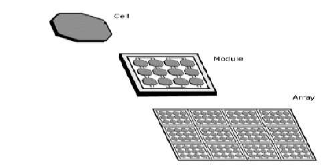
Fig. 2.Photovoltaic system.
An ideal is demonstrated by a current source in parallel with a diode. Still no solar cell is ideal and so shunt
and series resistances are added to it. 𝑅𝑠 Stands the intrinsic series resistance whose value is very small. 𝑅𝑝 Stands the
equivalent shunt resistance which has a very great value.
Relating Kirchhoff’s law to the node 𝐼𝑝ℎ where, diode, 𝑅𝑝 and 𝑅𝑠 meet, we get
𝐼𝑝ℎ = 𝐼𝑅𝑃 + 𝐼𝐷 + 𝐼 (1)
We get the succeeding equation for the
photovoltaic current
𝐼 = −𝐼𝑅𝑃 − 𝐼𝐷 + 𝐼𝑝ℎ (2)
Where, is the Insolation current, I is the Cell
current, 𝑅𝑝 stands the Parallel resistance, 𝑅𝑠 stands the series resistance. Photo current 𝐼𝑝ℎ of the photovoltaic
module be influenced by linearly on the solar irradiation
and is too influenced by the temperature according to the
succeeding equation:
𝐼𝑝ℎ = [𝐼𝑠𝑐𝑟 + Ki*(Tk − Tref)] ∗ λ/1000 (3)
𝑉𝑝𝑣 +( 𝐼𝑝𝑣 *𝑅𝑠 )/ 𝑅𝑠ℎ (5)
Where 𝑁𝑃 and 𝑁𝑠 are, respectively, the number of
parallel and Series networks of cells in the given
photovoltaic module 𝑉𝑝𝑣 =𝑉𝑜𝑐 =12V, 𝑅𝑠 stands the equivalent series resistance of the module, and 𝑅𝑝 stands the
equivalent parallel resistance.

The power circuit of a traditional SEPIC converter is shown in Fig. 3. The step-up and step-down static gains of SEPIC converter is an interesting operation characteristic for wide input voltage applications. The circuit diagram of SEPIC converter with voltage multiplier technique is shown in Fig. 4. The modified SEPIC converter is obtained by placing the capacitor C2 and diode D2 . Design parameters and the static gain of the traditional SEPIC converter are changed with this modification on topology.
Fig. 3.Traditional SEPIC converter.
In the modified SEPIC converter, the capacitor C2 is charged with the output voltage. Therefore, when the switch is conducting, the voltage applied to the inductor L2 is higher than the voltage obtained from a traditional SEPIC converter.
IJSER © 2015 http://www.ijser.org
International Journal of Scientific & Engineering Research, Volume 6, Issue 3, March-2015 544
ISSN 2229-5518
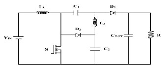
Fig. 4.Voltage multiplier SEPIC converter.
converter are compared with a traditional SEPIC converter and a boost converter. Theoretical waveforms of modified SEPIC converter is shown in Fig. 6.
At steady state, the average inductor voltage is zero. Hence, the relation for the inductor L1 is given by equation (6)
![]()
𝑇𝑜𝑛
𝑇𝑜𝑓𝑓
![]()
= (𝑣𝑐2 −𝑣𝑖𝑛)
𝑣𝑖𝑛
(6)
Assume modified SEPIC converter is operating in continuous conduction-mode operation. Based ON and OFF position of the switch S it consists of two modes of operation:
Mode-I [T0, T1]: At time T0, the switch S is in off state as
By cross multiplying equation (6), we get
𝑣𝑖𝑛 ∗ 𝑇𝑜𝑛 = (𝑣𝑐2 − 𝑣𝑖𝑛 ) ∗ 𝑇𝑜𝑓𝑓 (7)
Let assume
shown in Fig. 5(a). The energy stored in inductor L1 is transferred to the load through the diode D1 and capacitor
𝛼 =![]()
𝑇𝑜𝑛
𝑇
(8)
C1 , and also to the capacitor C2 through the diode D2 . Hence, voltage across capacitor C2 is equal to the voltage across switch. The energy which is stored in the inductor L2 is transferred to the load through the output diode D1 .
Mode-II [T1, T2]: At the time T1, switch S is in conduction as shown in Fig. 5(b). Diodes (D 1 & D2 ) are blocked, and inductors (L1 & L2 ) stores energy. The input voltage is applied to the inductor L1 and the voltage (VC1 – VC2 ) is
applied to inductor L2 . Hence the voltage across C2 is
Where αR is known as duty cycle, 𝑇𝑜𝑛 is known as on time, 𝑇𝑜𝑓𝑓 is known as off time and T is known as total time
period.
Substituting eq. (8) in equation (7), we get
𝑣𝑖𝑛 ∗ 𝛼 = (𝑣𝑐2 − 𝑣𝑖𝑛 ) ∗ (1 − 𝛼)R (9)
The relation between input voltage 𝑣𝑖𝑛 and voltage across
capacitor 𝑣𝐶2
greater than voltage across C1.
Ris represented in equation (10)
![]()
![]()
𝑣𝑐2 = 1
(10)
𝑣𝑖𝑛
(1−𝛼)

(a)
(b)
Fig. 5. Operation modes of converter. (a) W hen S in OFF state. (b) When S in ON state.
The theoretical analysis and design procedure obtained for a modified SEPIC converter is given in this section. The theoretical analysis of modified SEPIC
When the switch S is turned-off, both the diodes D 1
and D2 are in on state and the output voltage 𝑣𝑜𝑢𝑡 Ris given
by equation (11)
𝑣𝑜𝑢𝑡 = 𝑣𝐶2 + 𝑣𝐶1 (11)
By using volt-sec principle at steady state, voltage across
inductor L2 is zero. The following equations (12) and (13)
are obtained as follows
(𝑣𝐶2 − 𝑣𝐶1 ) ∗ 𝑇𝑜𝑛 = (𝑣𝑜𝑢𝑡 − 𝑣𝐶2 ) ∗ 𝑇𝑜𝑓𝑓 (12)
Substituting equation (8) in equation (10), we get
(𝑣𝐶2 − 𝑣𝐶1 ) ∗ (𝛼) = (𝑣𝑜𝑢𝑡 − 𝑣𝐶2 ) ∗ (1 − 𝛼)R (13)
The voltage across capacitor v𝑐1 is given in equation (12)
𝑣𝑐1 = 𝑣𝑜𝑢𝑡 − 𝑣𝐶2 (14)
Substituting eq. (10) and eq. (14) in eq. (11), gain of the
modified converter is given by equation (15),
IJSER © 2015 http://www.ijser.org
International Journal of Scientific & Engineering Research, Volume 6, Issue 3, March-2015 545
ISSN 2229-5518
![]()
![]()
𝑣𝑜𝑢𝑡 = (1+𝛼)

(15)
𝑉𝑖𝑛
(1−𝛼)
The static gain for this converter varies depending
on the duty cycle.
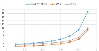
Gains with respect to various duty cycles of a traditional SEPIC converters, a modified SEPIC converter and a boost converter are presented in TABLE 1, 2 and 3. Expression for duty ratios of a traditional SEPIC, a modified SEPIC and a boost converter is given in the TABLE 4. Comparisons of gain with respect to various duty cycles for a modified SEPIC, a traditional SEPIC, a boost converter are shown in Fig.7.
TABLE 1
VARIATION IN GAINS FOR DIFFERENT DUTY
CYCLES FOR A TRADITIONAL SEPIC CONVERTER
Fig. 6.Theoretical waveforms of modified SEPIC converter.
TABLE 2
IJSER © 2015 http://www.ijser.org
International Journal of Scientific & Engineering Research, Volume 6, Issue 3, March-2015 546
ISSN 2229-5518
VARIATION IN GAINS FOR DIFFERENT DUTY CYCLES FOR A MODIFIED SEPIC CONVERTER![]()
Fig. 7.Variation in gains.
![]()
Duty cycle
TABLE 2
VARIATION IN GAINS FOR DIFFERENT DUTY CYCLES
Modified SEPIC converter has a better gain compared to a boost converter and a SEPIC converter. A
plot of variation in gains of a modified SEPIC, a boost and a traditional SEPIC converter is shown in Fig. 7 for a better understanding.
FOR A BOOST CONVERTER
The maximum input current ripple plays a vital
role in determining the input inductance. By using the function of maximum input current ripple, input inductance value is obtained. The equation for determining the input current ripple is same for boost, traditional SEPIC, and the modified SEPIC converters, input current ripple is
denoted as ∆I𝐿1 is given in (16) when the power switch is in
on state
(𝑣𝑖𝑛 ∗ 𝛼)![]()
∆𝐼𝐿1 = (𝐿
(16)
∗ 𝐹)
By cross multiplication of equation (16), we get
TABLE 4
COMPARISION OF DUTY CYCLE RATIOS
∆𝐼𝐿1
∗ 𝐹 ∗ 𝐿1
= 𝑣
𝑖𝑛
∗ 𝛼 (17)
Where F is the switching frequency.![]()
![]()
![]()
Input inductance value is equal to 1mH which is obtained from equation (19). The input inductance value is determined for the converter conducting at the peak of the
input voltage v𝑖𝑛 . At this operation point, converter has duty cycle of 𝛼 = 40 percent, the input voltage is equal to v𝑖𝑛
= 12 V, and the input current ripple ∆I𝐿1 considered by
taking (23/100) of the I𝑃𝐸𝐴𝐾 peak input current. Hence, the
input current ripple is obtained as follows![]()
23
∆I𝐿1 = I𝑃𝐸𝐴𝐾 ∗ 100 (18)
IJSER © 2015 http://www.ijser.org
International Journal of Scientific & Engineering Research, Volume 6, Issue 3, March-2015 547
ISSN 2229-5518
The calculated input inductance is equal to![]()
𝐿 = (v𝑖𝑛∗𝛼)
(19)
voltage(27.15V), the output capacitance is obtained by equation.
(𝐿1 ∗∆I𝐿1 ∗𝐹)
𝐶𝑜𝑢𝑡 =![]()
(𝑝𝑜𝑢𝑡 )
(25)
By substituting the values in equation (19) input inductance
value is given in (20)
𝐿1= 247 uH (20)
The input inductance value for inductor L1 = 247
uH. The inductance value for inductor L2 is equal to the inductance value for inductor L1 i.e., L2 = 247uH.
Here the capacitors C1 is known as series capacitor, C2 capacitor is known as the multiplier Capacitor. C2 changes with the input voltage and at the same time, capacitor C1 also changes with the input voltage. Capacitor
charge variation is denoted with ∆QcR. Circulating current
present in both capacitors C1 , C2 are equal. When the switch
is in conduction period, the current in the inductor L2
current is equal to the C2 and C1 capacitances. The capacitor
charge variation ∆QcR is given in (21)
∆Qc = (𝛼 ∗ ∆I𝐿1 ∗ 𝑇) (21)
Capacitor voltage ripple ∆V𝐶 is obtained by using
the relation Q=C*V is given in (22)
(∆Qc)
�2 ∗ 3.14 ∗ 𝐹𝑔 ∗ 2 ∗ 𝑣𝑜𝑢𝑡 ∆𝑉𝑜𝑢𝑡 �
By substituting the values in equation (25) output![]()
capacitance C𝑜𝑢𝑡 value is given in (26)
𝐶𝑜𝑢𝑡 = 1000𝑢 𝐹 (26)
The simulation results of PV fed modified SEPIC
converter are obtained for an input of 12V and the output of
27.15V, at 40 percent duty cycle with 14.15W power at
switching frequency of 25 KHz.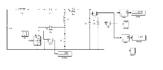
∆V𝐶 =![]()
(22) (C)
(a)

C1 and C2 capacitances both are having the same value is given below in equation (23)
(∆I𝐿2 ∗ 𝛼)![]()
C1 = C2 = (∆V
(23)
∗ 𝐹)
By substituting the values in equation (23)
capacitance value is given in (24)
= 1𝑢 𝐹 (24)
The capacitance values for C1 and C2 of the
modified SEPIC converter is equal to C1=C2= 1 uF.

The output capacitor C𝑜𝑢𝑡 is also known as filter
capacitor The output capacitance value depends mainly on
the supply frequency F𝑔 , the output power p𝑜𝑢𝑡 Rand the low frequency output voltage ripple∆V𝑜𝑢𝑡 .Taking an output
voltage ripple equal to (1/100) of the output
IJSER © 2015 http://www.ijser.org
(b)
(c)
(d)
International Journal of Scientific & Engineering Research, Volume 6, Issue 3, March-2015 548

ISSN 2229-5518
(e)

(f)

(g)

(h)
Fig. 8. Simulation results of modified SEPIC converter. (a) Mat lab model of modified SEPIC converter. (b) Mat lab model of modified SEPIC converter along with PV fed. (c) Input voltage waveform. (d)
Output voltage waveform. (e) Current through inductor 𝐿1 waveform. (f) Current through inductor 𝐿2 waveform. (g) Firing pulses across switch.
(h) Output current waveform.
TABLE 5
PARAMETERS OF MODIFIED SEPIC CONVERTER
Components | specifications |
INPUT VOLTAGE(Vin) | 12 V |
OUTPUT VOLTAGE(Vo) | 27.15V |
L1,L2 | 247 uH,247 uH |
C1,C2,Cout | 1 uF,1 uF,1000 uF |
LOAD RESISTOR(Ro) | 58 OHMS |
MOSFET | 1 |
DIODE(D1,D2) | 2 |
POWER | 14.1W |
DUTY CYCLE | 40% |
Parameters of modified SEPIC converter is shown in TABLE 5. Simulation results of modified SEPIC converter validates our study.
The simulation results of PV fed traditional SEPIC
converter are obtained for an input of 12V and the output of
7.79V, at 40 percent duty cycle with power rating of 3.9W at switching frequency of 25 KHz.
(a)

(b)


(c)

(d)

(e)
IJSER © 2015 http://www.ijser.org
International Journal of Scientific & Engineering Research, Volume 6, Issue 3, March-2015 549
ISSN 2229-5518
(f)


(g)
(h)
Fig. 9. Simulation results of traditional SEPIC converter. (a) Mat lab model of traditional SEPIC converter. (b) Mat lab model of traditional SEPIC converter along with PV fed. (c) Input voltage waveform. (d)
Output voltage waveform. (e) Current through inductor 𝐿1 waveform. (f) Current through inductor 𝐿2 waveform. (g) Firing pulses across switch.
(h) Output current waveform.
TABLE 6
PARAMETERS OF TRADITIONAL SEPIC CONVERTER
Parameters of traditional SEPIC converter is shown in TABLE 6. Simulation results of traditional SEPIC
converter validates our study.
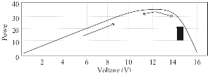
The effectiveness of a solar cell is very small. In directive to rise the efficiency, approaches are to be assumed to match the source and load correctly. One such technique is the Maximum Power Point Tracking (MPPT). This is a method used to achieve the extreme possible power from a variable source. There are various techniques used for maximum power point tracking a few are the Perturb and Observe (P&O), Incremental Conductance (IC), Fuzzy Logic, and so on. The P&O algorithm is very common and simple.
Fig. 10. Power graph for P and O algorithm.

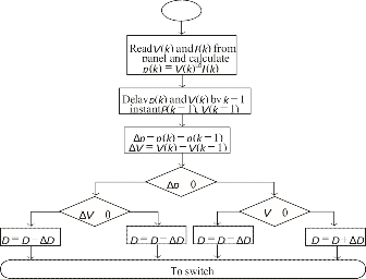
In P&O algorithm, a small perturbation (ΔD = 0.01) is introduced in the system. This perturbation origins the power of the solar module to vary. If the power increases due to the perturbation, then the perturbation is sustained (D + ΔD) in that direction. Once the peak power is reached, the power at the resulting instant decreases and afterwards that the perturbation reverses (D − ΔD).
PV module
PV pow MPPT lation
PWM
Fig. 11. DC-DC converter for operation at the MPPT.
With the deviation of irradiation and temperature, the power output of PV module differs constantly. The maximum power point tracking (MPPT) algorithm is used for extracting the maximum power from the solar PV
IJSER © 2015 http://www.ijser.org
International Journal of Scientific & Engineering Research, Volume 6, Issue 3, March-2015 550
ISSN 2229-5518

module and transfer that power to the load A DC-DC converter (step up/step down), aids the purpose of transmitting maximum power from the PV module to the load and performances as an interface among the load and the module.
Start
Fig. 12. Flow chart of P&O MPPT algorithm.
The simulation results of PV fed modified SEPIC converter with MPPT are obtained for an input of 12V and the output of 36.69V, at 50 percent duty cycle with 14.15W power at switching frequency of 25 KHz.
(a)

(b)
(c)
(d)

(e)
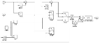
Fig. 13. Simulation results of modified SEPIC converter. (a) Mat lab model of modified SEPIC converter along with PV fed and MPPT controller. (b) Input voltage waveform. (c) Output voltage waveform. (d) MPPT Simulink block. (e) Firing pulses across switch.
From the results, it is clear that a modified SEPIC converter has higher circuit complexity than a SEPIC converter and a boost converter. The main advantage of modified SEPIC converter circuit it has high gain for a given duty cycle. The simulation results validates our study.
[1] M. G. Villalva, J. R. Gazoli, E. Ruppert F, "Comprehensive approach to modeling and simulation of photovoltaic arrays", IEEE Transactions on Power Electronics, 2009 vol. 25, no. 5, pp. 1198--1208, ISSN 0885-8993.
[2] M. G. Villalva, J. R. Gazoli, E. Ruppert F, "Modeling and circuit-based simulation of photovoltaic arrays", Brazilian Journal of Power Electronics, 2009 vol. 14, no. 1, pp. 35--45, ISSN 1414-8862.
[3] Mummadi Veerachary, "Control of TI-SEPIC Converter for
Optimal Utilization of PV Power", IICPE, 2010 New Delhi.
[4] R. Sridhar, Dr. Jeevananathan, N. Thamizh Selvan, Saikat
Banerjee,“Modeling of PV Array and Performance
IJSER © 2015 http://www.ijser.org
International Journal of Scientific & Engineering Research, Volume 6, Issue 3, March-2015 551
ISSN 2229-5518
Enhancement by MPPT Algorithm", International Journal of Computer Applications (0975 – 8887) Volume 7– No.5, September 2010.
[5] Hairul Nissah Zainudin, Saad Mekhilef, “Comparison Study of Maximum Power Point Tracker Techniques for PV Systems”, Cairo University, Egypt, December 19-21, 2010, Paper ID 278.
[6] Katherine A. Kim and Philip T. Krein, “Photovoltaic Converter Module Configurations for Maximum Power Point Operation”, University of Illinois Urbana-Champaign Urbana, IL 61801 USA.
[7] Huan-Liang Tsai, Ci-Siang Tu, and Yi-Jie Su, “Development of Generalized Photovoltaic Model Using MATLAB/SIMULINK”, Proceedings of the World Congress on Engineering and Computer Science 2008 WCECS 2008, October 22 - 24, 2008, San Francisco, USA.
[8] M. Berrera, A. Dolara, R. Faranda and S. Leva, “Experimental test of seven widely-adopted MPPT algorithms”, 2009 IEEE Bucharest Power Tech Conference,June 28th - July 2nd, Buchares
IJSER © 2015 http://www.ijser.org
International Journal of Scientific & Engineering Research, Volume 6, Issue 3, March-2015 552
ISSN 2229-5518
![]()
IJSER © 2015 http://www.ijser.org