International Journal of Scientific & Engineering Research, Volume 4, Issue 7, July-2013 1508
ISSN 2229-5518
Low Power Single Bit line 6T SRAM Cell
With High Read Stability
V.Subhamkari, G. S. Siva Kumar
Abstract— This paper presents a novel CMOS 6-transistorSRAM cell for different purposes including low power embedded SRAM applications and stand-alone SRAM applications. The data is retained by the cell with the help of leakage current and positive feedback, and does not use any
refresh cycle. The size of the new cell is comparable to the conventional six-transistor cell of same technology and design rules. Also, the proposed cells uses a single bit-line for both read and write purposes.
The cell proposed in this paper consumes less dynamic power and has higher read stability than the standard one. In conventional six- transistor (6T) SRAM cell, read stability is very low due to the voltage division between the access and driver transistors during read operation. In existing SRAM topologies of 8T, 9T and higher transistor count, the read static noise margin (SNM) is increased but size of the cell and power consumption increases relatively.
In the proposed technique, the SRAM cell operates by charging / discharging of a single bit-line (BL) during read and write operation, resulting in reduction of dynamic power consumption to only 40% to 60% (best case / worst case) of that of a conventional 6T SRAM cell. The power consumption is further decreased if the switching operational voltage of the bit-line lies between 0.25VDD to 0.5VDD. All simulations are done using 0.18um Technology.
Keywords- low power, read stable, single bit-line, SRAM, SNM, 6T Cell, acess and driver transistors.
1. INTRODUCTION
Exponential increase in VLSI fabrication process has resulted in the increase of the densities of Integrated Circuits by decreasing the device geometries. But devices with such high densities are susceptible to high power consumption and run time failures. Apart from such concerns, other factors such as a growing class of portable devices like PDA, cellular phones, portable multimedia devices etc have given designers a motivation to look into low power design and today, not only device geometries are a technology focus, but also reducing the existing topologies keeping the functionality intact is also a major area.
Memories are an integral part of most of the digital devices and hence reducing power consumption of memories as well as area reduction is very important as of today to improve system performance, efficiency and reliability. Most of the embedded and portable devices use SRAM cells because of their ease of use as well as low standby leakage.
A six-transistor SRAM cell (6T SRAM cell) is conventionally used as the memory cell.

Author: V. Subhamkari is currently pursuing Master of technology in Very large scale integration system design in pragati engg college,India PH:9985401995, E-mail: cherrysubbu@gmail.co m
Guide: G. S. Siva Kumar is currently working as assoc.professor in
Electronics and communications engineering dept at pragati engg
college.India PH:9949811979
However, the 6T SRAM cell produces a cell of larger size than that of a DRAM cell, resulting in a low memory density.
Therefore, conventional SRAM cells that use the 6T RAM cell have difficulty in meeting the growing demand of a larger memory capacity in mobile applications.Also the conventional six transistor (6T) SRAM cell shows poor stability at very small feature size with lowpower supply. During the read operation, the stability drastically decreases due to the voltage division between the access and driver transistors.
Considerable research work has been done over the past several years to design a low power SRAM cell, which also resulted in a significant degradation in SRAM cell data stability. With each technology generation, the scaling of CMOS devices results in random variations in the number of dopant atoms in the channel region of the device. This causes random variations in the device parameters like the threshold voltage (Vt ) and is usually known as random dopant fluctuation (RDF) [1].
Since SRAM cells operate on delicately balanced Transistors, and the conventional six transistor (6T) SRAM cell shows poor stability during read operation, it is very important to consider these issues during new memory cell designs.
IJSER © 2013 http://www.ijser.org
International Journal of Scientific & Engineering Research, Volume 4, Issue 7, July-2013 1509
ISSN 2229-5518
2. BACKGROUND
Rapid development of low power, low voltage SRAM cells has been experienced during recent years. This is due to an increasing demand of embedded devices, notebooks, laptops, hand held communication devices and IC memory cards. Due to these concerns limiting power consumption is a must and hence new techniques are being realized to improve energy efficiency at all levels of the design. In this paper an overall analysis has been carried-out for a novel SRAM cell with respect to stability and switching power consumption.
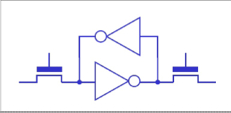
Figure 1: Traditional SRAM Cell With Dual Bit Line
In the traditional 6T-SRAM (Fig.1), the cells are expected to be both read stable and also writable and such functionality must be preserved for each cell under worst- case variation. At the cell level, the static noise margin and write margin are both maintained by the selection of calculated transistor strength ratios, which in turn presents conflicting constraints on the cell transistor strengths. For the cell stability during a read operation, the storage inverters are usually made strong and the pass-gates weak. Whereas the opposite is usually the case for cell write ability which is a weak storage inverter and strong pass-gates. Device variations common in nano-scale fabrication can severely impact this delicate balance of transistor strength ratios, which dramatically degrades stability and write margins. These problems are further exacerbated by low voltage operations as threshold voltage variation consumes a larger fraction of these voltage margins. Variability can thus limit the minimum operating voltage of SRAM [2].
Many design techniques circumventing variability problems have been proposed to enable low-voltage operation of 6T cells. One such method is the addition of a second higher supply voltage dedicated to the SRAM array which is very effective and ensures sufficient margins with scaling of the logic supply voltage. The SRAM voltage does not scale with technology in such cases and could even be increased as variability intensifies. Instead of being tied to a fixed higher supply, dynamically modulated supplies could
also be used with SRAM arrays that are pulsed to different levels when a read or write event occurs. To an extent, this helps decoupling read and write events from the standby condition such that the optimum bias conditions can be used in each case. Such techniques may add complexity to the design, but can be used to improve cell stability and write-ability or standby leakage. These methods may reduce the trade-offs between cell optimization for read and write but cannot eliminate them as a whole.
Conflicting needs of cell read stability and write-ability compromises the variability tolerance of a 6T standard cell. Balanced conditions are used for the same pass-gate devices for reading and writing the cell, and it is inevitable that the two conditions cannot be simultaneously optimized. Similar to the dynamically modulated power supplies which separate requirements for reading and writing, a SRAM cell can also achieve that by modifying itself. A write operation to an unselected column of a 6T standard SRAM cell can result in stability issues, when the word line is activated while both bit lines are held high; a bias condition similar to a read operation. Such problems resulted in design of different topologies of SRAM cell to improve the data stability and leakage power consumption [3]
3. PROPOSED 6T SRAM CELL
The proposed design has increased the read stability and SNM, without affecting the Size or Power Consumption of a Standard 6 Transistor SRAM cell.
3.1. Minimization of a 6T Standard Cell
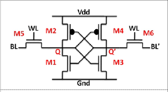
Figure 2: 6 Transistor Standard SRAM Cell
The schematic of Fig 2 once again shows the 6 Transistor SRAM cell which uses two bit-lines and one word-lines (tied to two acess transistors)
IJSER © 2013 http://www.ijser.org
International Journal of Scientific & Engineering Research, Volume 4, Issue 7, July-2013 1510
ISSN 2229-5518
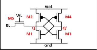
Figure 3: 5 Transistor (Single Ended) SRAM Cell
With the Transistor M6 being taken away a schematic like
Fig 3 is obtained, which still functions like the 6T SRAM but
the advantages of this design are reduction in cell area and power consumption. The cell area decreases by one transistor and one bit line. The power consumption from charging the bit line decreases by approximately a factor of 2 because only one bit line is charged during a read operation instead of two, and the bit line is charged during a write operation about half of the time (assume equal probability of writing 0 and 1) instead of every time when a write operation is required.

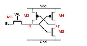
Figure 4: Transistor (Single Ended) SRAM Cell
With the Transistor M1 being taken away a schematic With the Transistor M1 being taken away a schematic like Fig 4 if obtained, which has the functionality of a SRAM and the main advantage of this design is the further reduction power consumption. Other advantages include significant larger write margin and smaller delay for writing 1, and slightly smaller cell area

3.2. The Proposed 6T New SRAM Cell
Figure 5: 6 Transistor(Single Ended)SRAM Cell(Proposed) The proposed 6 Transistor new SRAM Cell is created
by adding two more transistors MRA (Read Access Transistor) and MRD (Read Driver Transistor) which shall work independently during read operation and won’t affect the Cell SNM in any way.
3.3. Memory Cell Operations
• Hold: If the cell content is a 1 (Q=VDD, Q’=0), bothmemory nodes will lock each other at their respective voltages. However, if the cell content is a 0 (Q=0, Q’= VDD), Q is floating. Referring to Fig
5, the leakage current through M5 must be greater
than that of M2 to ensure Q stays at 0. Fortunately, since NMOS (M5) is a stronger current driver than PMOS (M2), this condition is satisfied.
• Write: The word-line WL is charged to VDD as in
6TStandard SRAM. Since NMOS is a stronger driver than PMOS, no problem is incurred while writing a 0 into the cell. The absence of the pull down NMOS for memory node Q allows writing a
1 into the cell easily. Writing a 1 is done by pre-
charging bit-line BL to VDD. While writing 0, the bit-line BL is discharged and then word-line WL is charged to VDD as in 6T Standard SRAM.
• Read: Considering the case of reading Q=0; beforereading a value from the storage nodes, the bit line BL is pre-charged to VDD. The read word line RL is then asserted to VDD. The storage node
IJSER © 2013 http://www.ijser.org
International Journal of Scientific & Engineering Research, Volume 4, Issue 7, July-2013 1511
ISSN 2229-5518
Q' that stores a 1 is statically connected to the gate of
MRA (Read Access Transistor) and will drain the
charges on the bit line through MRD to GND as the
RL is 1, which means that the bit line has just read a
0. On the contrary, when Q=1, Q' will be 0 and MRA will be in cutoff and the bit line BL would not be able to discharge through MRD to Gnd, and it would read a 1.
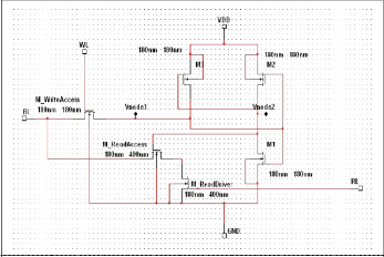
Figure 6: schematic Proposed 6T SRAM Cell in Multisim
4. SIMULATION RESULTS
4.1. Dynamic Power Consumption
In an SRAM operation, power is consumed in two phases:
the setup phase and the operation phase.
Energy consumed during the setup phase is dominated by pre-charging/discharging various buses such as bit lines andword lines. Using the formula Eline = 0.5 * Cline * Vline2, in which Cline is the line capacitance and Vline is the change in linevoltage, the energy drawn from the supply by the bus can be calculated. From this information, the average power of an SRAM operation is obtained by dividing the clock period, assuming that each SRAM cell can only perform one operation per clock period, and all word lines and bit lines are discharged to 0 after performing each operation. Also the clock has 50% duty cycle. In the simulation performed, a clock with 40ns clock period is used (or equivalent to 25MHz clock frequency and 1pF bit-line capacitance).
Therefore, consumed power Pline = Cline * Vline2 * F Dynamic power dissipation can be lowered by reducing the
switching activity and clock frequency but it affects
theperformance . Reduction of supply voltage leads to degradation of the cell data stability. Hence dynamic power
dissipation can be lowered by reducing bit-line capacitance of the SRAM cell without degrading the performance [9].
Power consumed during the operation phase is dominated by active power and leakage power. Active power is the power consumed when both pull-up and pull- down networks are active, creating a direct current path from VDD to ground. Leakage power is the power consumed when charges “leak” through a transistor that is off.
TABLE I.CALCULATED SWITCHING POWER Charging and Discharging of only Bit-Line considered
| 6T Standard SRAM Cell | Proposed 6T SRAM Cell |
WRITE 0 | 162uW | 0uW |
WRITE 1 | 162uW | 81uW |
READ 0 | 243uW | 162uW |
READ 1 | 243uW | 81uW |
For every write operation of a 6T Standard Cell, the complementary data is placed on both the bit-lines and then the pre-charge circuit is activated. Only one of the bit-lines gets charged depending on the data value. Once the write is completed, it is assumed that the capacitor is discharged. So power dissipation happens twice during a write phase. During a read cycle, again both the bit-lines are charged and then one is discharged during reading a Zero, while the other is discharged after the operation is complete.
For the proposed 6T SRAM Cell, only a single bit-line is either charged if it is a 1 or does not get charged at all assuming that the data was already present before the pre- charge circuit has been activated. After the write 1 operation, the bit-line is assumed to get discharged. During a read 0 cycle, the bit-line capacitance is pre-charged and discharged through the cell, where as in a read 1 cycle, the bit-line is pre-charged and assumed to be discharged after the read process is over.
4.2. Delay Calculation
SRAM delays are usually defined as the time it takes to read or write a value from an SRAM cell. When a node is
IJSER © 2013 http://www.ijser.org
International Journal of Scientific & Engineering Research, Volume 4, Issue 7, July-2013 1512
ISSN 2229-5518
switching, delay is measured as the time difference between
10% and 90% of the voltage swing. For example, if node A is
being changed over from 0V to 1.8V, then the delay is the time node A takes to go from 0.18V to 1.62V.
In the simulation, it is assumed that the bit-line(s) have
1pF capacitance which is much higher a value than node
capacitance at VNode1. Therefore, it takes much less effort to switch memory nodes than to switch bit line. This is why, in general, delays for write operation are smaller than that of read operation in SRAMs, because writing into a cell is the same as switching the memory node, and reading from a cell is the
same as switching the bit line. Note that for read operation, since the bit line is pre-charged to VDD, there is no significant current flow and voltage changes across the access transistor if the cell contains a 1. Therefore, read 1 delay is not defined.
The proposed 6T SRAM Cell has the smallest write 1 delays because there is no pull-down NMOS that keeps the memory node from being pulled up to VDD. For the same reason, it also has the worst write 0 delays, because there is no pull-down NMOS that helps to bring the memory node to
0.
TABLE II. DELAY ANALYSIS RESULTS
Simulation Results from Multisim 11
| 6T Standard SRAM Cell | Proposed 6T SRAM Cell |
WRITE 0 | 5.1 nS | 6nS |
WRITE 1 | 5.5 nS | 0nS |
READ 0 | 7.5nS | 8.5nS @ 600nM 6.5nS @ 800nM {MRD/MRA} |
4.3. Static Noise Margin
SRAM cell design has to achieve high integration density nowadays and it has led to a stringent constraint on the cell area in modern embedded systems or memory modules. Choosing minimal width-to-length ratios for the SRAM cell transistors is the first step to achieve such a design. As previously mentioned, variations in the threshold voltage Vth, increase steadily due to random dopant density fluctuations in channel, source and drain as the dimensions scale down to nanometer regime [11]. Therefore, differences are common, between two closely placed transistors which
were supposed to be identical. The differences are mainly in their their electrical parameters such as Vth and make
the design of the SRAM less predictable and controllable. Moreover, the stability of the SRAM cell is seriously affected by the increase in variability and by the decrease in supply voltage Vdd. Considerable research in understanding and modeling the stability of the SRAM cell has been done in the past. Development of several analytical models of the static noise margin (SNM) have been done in the past. Each of the work tried to optimize the design of the cell, to forecast the effect of parameter changes on the SNM [12] and to estimate the impact of intrinsic parameter variations on the cell stability [13]. Further, maximization of cell stability has been done in new SRAM cell circuit for future technology nodes [14].
The data retention of the Standard 6T SRAM cell in hold state and the read state are important constraints in advanced technologies. The cell becomes less stable at low VDD, with increase in leakage currents and increasing variability. “The stability is usually defined by the static noise margin as the maximum value of the DC noise voltage that can be tolerated by the SRAM cell without altering the stored bits [15].”
In the standard 6T SRAM cell the read static-noise- margin (SNM) is much affected with decrease in supply voltage (VDD) and transistor mismatch,. This mismatch [12], [16] happens due to variations in physical quantities the devices designed to be identical. Commonly known physical quantitiesare threshold voltages, body factor and current factor. Though SNM decreases at low VDD the overall delay of the SRAM increases and also data destruction takes place with low VDD read operation in SRAM cells [12]. But in the proposed SRAM cell, reading from the cell has no effect on the static noise margin because the data retention and the data output blocks are isolated.
The main operations of the SRAM cell are the write, read and hold. The static noise margin is certainly more important at hold and read operations [6] , specifically in read operation when the wordline is 1 and the bitlines are precharged to 1. The internal node of SRAM which stores 0 will be pulled up through the access transistor across the access transistor and the driver transistor. This increase in voltage severely degrades the SNM during read operation
IJSER © 2013 http://www.ijser.org
International Journal of Scientific & Engineering Research, Volume 4, Issue 7, July-2013 1513
ISSN 2229-5518
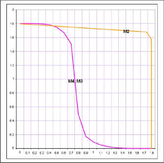
Figure 7. Hold State SNM Curve for the proposed 6T Cell
During read/hold operation, the requirement is that the SRAM cell must be as robust as possible so that a sudden disturbance will not change the content in the memory nodes. For example, read noise margin of 200mV means that during read operation, if one of the memory nodes (Q or Q’) changes by less than 200mV, then we can be sure that after the read operation, the content of Q and Q’ will remain the same, and any disturbance to the voltage in the cell will be eliminated. Therefore, a larger read/hold noise margin is preferred. During write operation, the situation is reversed; the requirement is to switch the content of Q and Q’ easily. Therefore, the write noise margin (more commonly referred to as the “write margin”) is defined as the range of voltage disturbances that will flip the content of the memory nodes. For example, if write margin is
500mV, then a range of at least 500mV disturbance in the memory nodes will cause their content to flip, thus achieving write operation.
It can be deduced from Fig 7 that Q’ is very zero stable where as Q is pretty much 1 stable. And the risk is that a mere 100mV of noise at Q’ when Q’ is at 1, can easily flip the state. But it is very unlikely that a noise can flip Q’ from
0 to 1
4.4. Improving Noise Margin – Dual Vt
The static noise margin at Hold State is very low as seen in Fig 7 and a slight disturbance of as less as 100mV at Q' can flip the state of the Cell. To prevent this from
happening, a higher Vt for M2 of Fig 5 can be implemented.
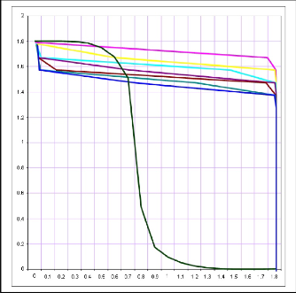
Figure 8. The SNM Curve plotted for different VBS
changing from 0.0V to 1.8V in steps of 300mV
It can be seen that the risk of Q’=1 being flipped with a little noise reduces with increasing VBS for M2 of Fig 5.
5. CONCLUSION
Continuing technology scaling puts a limit on how much supply voltage can be scaled. Therefore, limiting the power consumption with new architectures are the design requirements in recent integrated circuits. In the case of SRAM, one seemingly counter intuitive approach is to utilize only a single bit-line without jeopardizing read stability, which leads to the development of a Single Ended
6T SRAM. The new SRAM operating scheme, gives a significant power reduction by reducing the amount of switching on bit lines. Extending this operating scheme also allows us to propose a single bit line design that achieves a relatively smaller area while retaining all of the power saving advantages. For a small penalty in delay, Single Ended 6T SRAMs are attractive alternatives as memory storage for applications that do not require high clock frequency. Although, higher operating frequency may be obtained by lowering the bit-line capacitance in the order of Femto Farads, instead of the 1pF, as assumed in this paper.
IJSER © 2013 http://www.ijser.org
International Journal of Scientific & Engineering Research, Volume 4, Issue 7, July-2013 1514
ISSN 2229-5518
REFERENCES
[1] S. Borkar, T. Karnik, S. Narendra, J.T schanz, A.
Keshavarzi, and V.de, “Parameter Variations and
Impact on Circuits & Microarchitecture," Proceedings of Design Automation Conerence., pp. 338-342, Jun.2003
[2] Jawar Singh, DhirajK.Pradhan et al,” A single ended 6T SRAM cell design for ultra low voltage applications”,IEICE Electronic Express,2008,pp-750-755
[3] Yen Chen,Gary Chen et al., “A 0.6V dual rail compiler SRAM design on 45nm CMOS technology with Adaptive SRAM power for lower Vdd_minVLSIs,Solid-State Circuits, IEEE Journal,vol.
44 ,April.2009, Issue 4 , pp.1209-1214
[4] Koichi Takeda et al, “A Read Static Noise Margin Free SRAM cell for Low Vdd and High Speed Applications”,Solid-State Circuits, IEEE Journal vol. 41, Jan.2006, Issue 1 , pp.113-121
[5] Aly, R.E. Bayoumi, M.A., “Low-Power Cache Design Using 7T SRAM Cell” Circuits and Systems II: Express Briefs, IEEE Transactions, vol. 54 April 2007, Issue: 4, pp. 318-322
[6] Benton H. Calhoun Anantha P. Chandrakasan “A 256- kb 65-nm Sub-threshold SRAM Design for Ultra-Low- Voltage Operation”,Solid-State Circuits, IEEE Journal vol. 42, March 2007, Issue 3 , pp.680-688.
[7] Peter Geens, WimDehaene, “A dual port dual width
90nm SRAM with guaranteed data retention at minimal standby supply voltage”,34th European Solid- State Circuits Conference, 2008. ESSCIRC 2008.pp-290-
293.
[8] FarshadMoradietal., “65nm Sub threshold 11 T SRAM
for ultra low voltage Application ,IEEE xplore,2008,pp-
113-117
[9] Dake Liu, and ChristerSvenson, “Power Consumption Estimation in CMOS VLSI Chips," IEEE Journal of Solid State Circuits, vol. 29, No. 6, pp. 663-670, June
1994
[10] K. Itohet. al., “Trends in Low-Power RAM Circuit Technologies”, Proceedings of the IEEE, pp.524-543, April 1995
[11] B. Cheng et al., “The impact of random doping effects on CMOS SRAM cell,” in Proc. ESSCIRC, Sep. 2004, pp. 219–222
[12] E. Seevinck et al., “Static-noise margin analysis of MOS SRAM cells,” IEEE J. Solid-State Circuits, vol. SC-22, no. 5, pp. 748–754, Oct. 1987
[13] J. Bhavnagarwala et al., “The impact of intrinsic device fluctuations on CMOS SRAM cell stability,” IEEE J. Solid-State Circuits, vol. 36, no. 4, pp. 658–665, Apr.
2001
[14] L. Chang et al., “Stable SRAM cell design for the 32 nm node and beyond,” in Symp. VLSI Technology Dig. Tech. Papers, Jun. 2005, pp. 128–129
[15] Evelyn Grossar, Michele Stucchi, Karen Maex, Member, IEEE, and WimDehaene, Senior Member, “Read stability and write-ability analysis of SRAM Cells for nanometer Technologies” IEEE Journal Of Solid-State Circuits, Vol. 41, No. 11, November 2006.
[16] Koichi Takeda, Yasuhiko Hagihara, Yoshiharu Aimoto, Masahiro Nomura, Member, IEEE, YoetsuNakazawa, Toshio Ishii, and Hiroyuki Kobatake, “A readstatic- noise-margin-free SRAM cell for low-VDD and high- speed applications,” in IEEE ISSCC Dig. Tech. Papers, Feb. 2005, pp. 478–479.
[17] Ultra-Low Voltage Nano-Scale Memories, Itoh, Kiyoo; Horiguchi, Masashi; Tanaka, Hitoshi (Eds.), Springer Publications
[18] Digital Integrated Circuits A Design Perspective, Second Edition, Jan M. Rabaey, AnanthaChandrakasan, BorivojeNikolic, Prentice-Hall
/ Pearson Publications
[19] Shilpi Birla, Neeraj Kr. Shukla, ManishaPattanaik, R.K.Singh, “Device and Circuit Design Challenges for Low Leakage SRAM for Ultra Low Power Applications”, Canadian Journal on Electrical & Electronics Engineering Vol. 1, No. 7, December 2010,
[20] Shilpi Birla, NeerajKr.Shukla, ManishaPattnaik, R.K.Singh “ANALYSIS OF THE DATA STABILITY AND LEAKAGE POWER IN THE VARIOUS SRAM CELLS TOPOLOGIES”, International Journal of Engineering Science and Technology, Vol. 2(7), 2010,
2936-2944
IJSER © 2013 http://www.ijser.org