International Journal of Scientific & Engineering Research, Volume 3, Issue 11, November-2012 1
ISSN 2229-5518
Low Power Explicit Pulsed Conditional Discharge
Double Edge Triggered Flip-Flop
Ms. Tania Gupta, Mr. Rajesh Mehra
Abstract— An explicit pulsed double edge triggered sense amplifier flip-flop for the low power and low delay is presented in this paper. The redundant transitions are eliminated by using the conditional technique named conditional discharge technique. By using the fast improved version of the nickolic latch along with the sense amplifier approach for the latching and the sensing stage the delay factor of the circuit is improved. Simulation using TSPICE and a 0.18µm CMOS technology shows that the proposed design has low power dissipation and small delay as compared to the existing design which use a conditional precharge technique in the design for removing the redundant transitions. Comparing with the previous work of the dual edge triggered flip-flops, the proposed one saved power upto 20.7%. The delay factor is improved by the factor of the 26.5% as compared to the existing design of the flip-flop.
Index Terms— Dual Edge Triggered Flip-Flop, Conditional Discharge, Conditional Prechrage, CMOS design, Explicit Pulsed, Sense
Amplifier
1 INTRODUCTION
—————————— ——————————
WITH the widespread use of the mobile devices in modern society, power efficiency and energy savings becomes the crit- ical issues for designers. Normally the high performance chips have high integration density and high clock frequency, which tend to dictate power consumption [1]. Consumer desire has caused a demand for ever increasing the number of portable applications requiring low power and high throughput. As more transistors are integrated with each new technology, leakage energy is also going to dominate the dynamic power consumption.
CMOS has been the dominant technology for very large scale integration (VLSI) implementations. As VLSI cir- cuits continue to grow and technologies evolve, the level of integration is increased and higher clock speeds are achieved. Higher clock speeds, increased levels of integration and tech- nology scaling are causing unabated increases in power con- sumption. Flip-flops are the critical timing elements which has a large impact on the circuit speed and power dissipation of the system. Clock related power consumption is 30-60% [2] of the total chip power i.e. this much power is dissipated by the clock distribution circuit out of total chip power. From this clock distribution power 90% is consumed by last part of the clock distribution network. There are basically four sources of power dissipation digital CMOS circuits which is the switch- ing power, short circuit power, leakage power and the static power [3]. In the digital circuits, the power dissipation on the signal switching (dynamic) is dominant.
. The switching power is given by formula given in equation 1.
P=αfCV2 (1)
Where α is the switching activity, f is the frequency and C is
the capacitance and V is the supply voltage. From the equation
1 it is clear that decreasing the supply voltage has a quadratic effect on decreasing the power dissipation P. But decreasing
the supply voltage beyond the certain limit will result in ex- ponential increase in the leakage current. Capacitances are affected by the characteristics of the devices [4]. Thus, the power can be reduced by decreasing the clock frequency. Dual edge clocking can be used to save half of the power on the clock distribution network. The power of the clocking system is given by the sum of the power consumed by the clock dis- tribution network and the power consumed by the flip-flops. Cutting the frequency of the clock by half the power is re- duced by the half on the clock distribution network. Flip-Flops are used as a main part of the digital synchronous circuit [5]. Mostly it is a part of computational circuits or used as registers in the pipeline structure to store the data for the further pro- cessing.

A single edge triggered flip-flop which is able to store a one bit. It takes the data on the one edge of the clock pulse either on rising edge or falling edge of the clock. As shown in the figure1 the two latches are used connected in series. At a one edge of the clock pulse only one latch is worked other latch is not worked. Means it takes only one edge of the clock pulse edge trig
Figur lop
IJSER © 2012
http://www.ijser.org
International Journal of Scientific & Engineering Research, Volume 3, Issue 11, November-2012 2
ISSN 2229-5518

In the double edge triggered flip-flop the latch takes the data on the both edges of the clock pulse. The basic block diagram of the dual edge triggered flip-flop is shown in the figure 2. This is basically master slave latch type dual edge triggered flip-flop. In this two latches connected in parallel. Both latches are work simultaneously. If the upper latch takes the data on the positive edge of the clock then at the same time lower latch takes the data on the negative edge of the clock, and the mul- tiplexer is used to combine the output of both to produce the final output.
Figure3. Clocking Scheme used for Dual Edge Triggering
Figure2. Schematic diagram of single edge triggered flip-flop
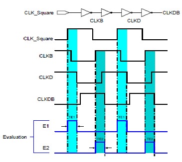
There are many types of the dual edge triggered flip-flop. Master slave latch dual edge triggered flip-flop, pulse trig- gered flip-flop. In Master salve latch flip-flop there is a dupli- cating of the latch part one is master part and other is for slave part. Thus there is a duplicating of the latch part. In pulse trig- gered flip-flop, there is implicit pulse triggered flip-flop and explicit pulse triggered flip-flop. In the implicit type flip-flop, the pulse generator used to generate the clock pulse is used inside the flip-flop circuitry. As the generation of the clock pulse inside the flip-flop, thus this clock pulse is not used by the neighbouring flip-flops. In the explicit pulse triggered flip- flop generation of the clock pulse outside the flip-flop. As the clock pulse generator outside the flip-flop, thus the generated clock pulse can be used by the multiple neighbouring flip- flops. The clocking scheme used for dual edge triggering in the dual edge triggered flip-flop is given in the figure 3. Firstly the CLK_Square is applied at the input of the inverter, CLKB and CLKD is the delayed version the CLK_Square. The shad- owed region represent the period at which the output is eval- uated [7] i.e. the actual logic response is determined. TE1 (Evaluation Period 1) represent the period of evaluation at rising edge of the clock signal and TE2 (Evaluation Period 2) for the falling edge of the clock.
2 EXISTING DUAL EDGE TRIGGERED FLIP-FLOP
In the dual edge triggered flip-flop basically consists of pulse generator stage, sensing stage and latching stage of the flip- flop. Pulse generator stage is used for the generation of the clock pulse of short period which is active at both rising edge and falling edge of the clock. The next stage is the sensing stage in which the data input (D) is sensed. In this sense am- plifier approach is used for sensing the input. The last stage is latching [8] stage in which output is latched and produces the final output Q and QB (complemented version of the Q).
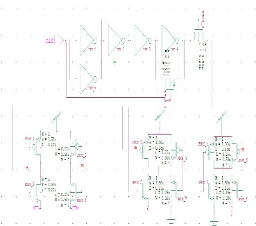
As the dual edge triggering is used in the circuit thus the power is saved by half as compared to the single edge triggered flip-flop. But a lot of power is consumed at the major internal nodes of the flip-flop. The reason for the power con- sumption at internal nodes is if the input is high for a long time then there is no significant change at the output. But if the input is high for long time means that there is charging and discharging at the internal nodes and produce the same result. To avoid this unnecessary charging and discharging at major internal nodes the conditional technique is used. In this existing design conditional precharge technique is used. In this technique a PMOS transistor is embedded in the control path of the circuit for disabling the charging of at the initial stage. This results in improve the power dissipiation of the whole circuit. The sechmatic diagram of this existing flip-flop is shown in figure 4.
IJSER © 2012
http://www.ijser.org
International Journal of Scientific & Engineering Research, Volume 3, Issue 11, November-2012 3
ISSN 2229-5518
stage NMOS transistor is embedded in the discharging path for avoiding the unnecessary charging and discharging at the major internal nodes. In the last stage fast symmetrical latch is used to improve the speed of the circuit. The power consump- tion in this case is reduced as compared to the existing circuit. The delay factor is also improved in this design as compared to the existing design. In this flip-flop design the conditional technique which is used for avoiding the power dissipation at major internal nodes.
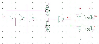
Figure4. Schematic Diagram of Existing Dual Edge Triggered
Flip-Flop
In this schematic diagram firstly the pulse generator part is used to generate the dual edge triggered clock pulse which is enable at both positive and negative edge of the clock pulse i.e. it is synchronised at both rising and falling edge of the clock pulse. The pulse generator can be shared by the multiple flip-flop circuits when the group of flip-flops are located close- ly because the explicit pulse generator is used. For this pur- pose inverter chain is used for produce the delayed version of the clock pulse. After that sensing stage is used, which is sense amplifier based flip-flop. When the input (D) applied at the PMOS_1 of circuit is low, SB will be set to high and if D is high, RB will be set to high. Therefore in this way conditional precharging technique is applied in the sensing stage of the dual edge triggered flip-flop, to avoid the redundant transi- tions at major internal nodes.two input controlled pMOS tran- sistors, PMOS_1 and PMOS_2 are embedded precharge paths of nodes SB and RB respectively. In the last satge fast symmet- rical latch is used the new latch makes use of SB and RB to pull up the output nodes.
3. PROPOSED DUAL EDGE TRIGGERED FLIP-FLOP
In the proposed design of the double edge triggered flip-flop explicit pulse generator is used for the generation of the clock pulse which generates a clock pulse of short period. After that sensing stage is used for sensing the input signal and the last one is latching stage to hold the data. The schematic diagram of the flip-flop is shown in figure 5 ans figure6. In the figure 5 pulse generator and the sensing stage is shown. Firstly, the pulse generator stage for generation of the clock pulse, after that sensing stage is used for sensing the data input. In this
Figure5. Schematic Diagram of Pulse Generator and Sensing
Stage of Proposed Dual Edge Triggered Flip-Flop
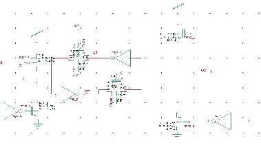
Figure6. Schematic Diagram of Latching Stage of Proposed
Dual Edge Triggered Flip-Flop
5 SIMULATION RESULTS
To evaluate the performance of the proposed flip-flop, comparison had been performed with the existing dual edge triggered flip-flop. All the flip-flops are designed using the Tanner EDA 13.1 Tools with 0.18 µm CMOS technology at an operating temperature of 270C and supply voltage of 1.8 V. The clock frequency which is used is 250 MHz.
In the figure 7 analog simulation of the existing design of the dual edge flip-flop is shown. in this waveform pulse sig- nal, data input, internal nodes SB and RB and output Q is shown (from bottom to top). In this pulse produced by pulse generator is shown which is active at both rising and falling edge of the flip-flop. The data input D is generated and then internal RB and SB are exactly complemented each other. At
IJSER © 2012
http://www.ijser.org
International Journal of Scientific & Engineering Research, Volume 3, Issue 11, November-2012 4
ISSN 2229-5518
the last output Q is shown which is high when the data input is high according to the clock pulse.
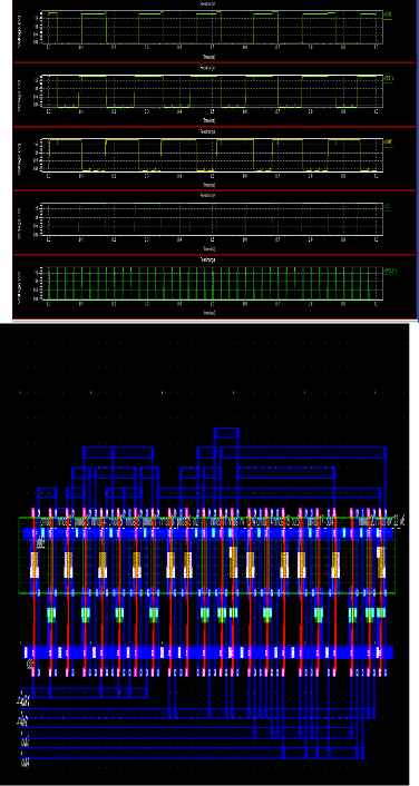
Figure8. Layout Design of Existing Dual Egde Triggered flip- flop design
The layout design of the proposed circuit is shoen in the figure
8. Layout is the general concept that describes the geometric
representation of the circuits by the means of the layers and
polygons. Different logical layers are used by the designers to generate the layout. There are specific layers for metal, polysil-
icon, contacts or diffusion areas. In this red color shows pol-
ysilicon, green color shown n+ diffusion, light green color shows p+ diffusion, light blue color shows metal1 and dark blue color shows metal 2.
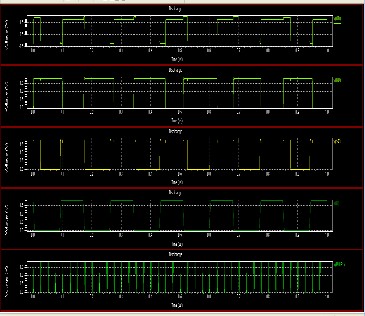
The analog simulation of the proposed circuit is shown in the figure 9. Firstly pulse produced from the pulse generator is shown, then the data input D, internal nodes SB and RB are shown and at the last output Q is shown in the waveform (from bottom to top).
Figure9. . Analog Simulation waveform of Proposed Dual
Edge Triggered Flip-Flop
The layout design of the proposed circuit is shown in the figure 10. Red color indicates the polysilicon, green color for n+ polysilicon, olive for the p+ diffusion and blue color for metal.
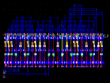
Figure10. Layout Design of Proposed Dual Egde Triggered flip-flop design
IJSER © 2012
http://www.ijser.org
International Journal of Scientific & Engineering Research, Volume 3, Issue 11, November-2012 5
ISSN 2229-5518
The comparison table of the existing design and the proposed design are shown below in table1 for different parameters.
TABLE 1
PERFORMANCE COMPARISON OF FLIP-FLOPS
As shown in the table, in the proposed design of dual edge triggered flip-flop, the power factor is improved by the factor of the 20.7% and the delay factor is improved by the factor of the
26.5% as compared to the existing design. the average current component is reduced in proposed circuit by the factor 26.77 %.
6 CONCLUSION
This paper presents dual edge triggered flip-flop for low pow- er and high performance flip-flop. The proposed dual edge trig- gered flip-flop achieves a low power by implementing dual edge triggering and conditional discharging technique. Dual edge trig- gering reducing the power dissipiation by half while paying vir- tually no penalty in the throughput. It also minimizes the latency factor by utilizing the improved fast symmetrical latch. The pow- er factor of the proposed flip-flop design is improved by the fac- tor 20.77%. The delay factor is also improved by the factor of
26.5% by using the TSPICE simulation with 0.18µm CMOS tech- nology.
7 ACKNOWLEDGEMENTS
Our thanks to the experts who have contributed in my pro- ject work ansd also want to thanks the NITTTR College provides me to the software tools for this work.
8. References
[1] Wai Chung, Timothy Lo, and Manoj Sachdev, “A Comparative Analysis of Low-Power Low-Voltage Dual-Edge-Triggered Flip- Flops”, IEEE Transactions on Very Large Scale Integration (VLSI) Systems, Vol. 10, No. 6, pp. 913-918, December 2002
[2] Peiyi Zhao, Jason Mcneely, Pradeep Golconda, Magdy A. Bayoumi, Robert A. Barcenas, Weidong Kuang, “Low-Power Clock Branch Sharing Double Edge Triggered Flip-Flop”, IEEE Transactions on VLSI Systems, Vol. 15, No. 3, pp. 338-345, March 2007.
[3] Xiaowen Wang, William H. Robinson, “A Low Power Double Edge
Triggered Flip-Flop with Transmission Gates and Clock Gating”,
IEEE International Midwest Symposium on Circuits and Systems
(MWSCAS), pp. 205-208, August 2010
[4] Y. T. Liu, L. Y. Chiou, and S. J. Chang, “Energy-Efficient Adaptive Clocking Dual Edge Sense Amplifier Flip-Flop”, IEEE International Symposium Circuits Systems (ISCAS), pp. 4329–4332, May 2006.
[5] Vladimir Stojanovic and Vojin G. Oklobdzija, “Comparative Analysis of Master–Slave Latches and Flip-Flops for High-Performance and Low-Power Systems”, IEEE Journal of Solid State Circuits, Vol. 34, Is- sue 4, pp. 536-548, April 1999.
[6] Rafael Peset Llopis and Manoj Sachdev, “Low Power testable Dual Edge Triggered Flip-Flops”, IEEE International Symposium on Low Power Electronics and Design (ISLPED), pp. 341-345, August 1996
[7] S.E.Esmaeili, A.J.AL.Khalili, G.E.R.Cowan, “Dual-edge Triggered Energy Recovery DCCER Flip-Flop for Low Energy Applications”, European Conference on Circuit Theory and Design (ECCTD), pp.
57-60, IEEE-2009
[8] Myint Wai Phyu, Kangkang Fu, Wang Ling Goh, Kiat-Seng Yeo, “Power Efficient Explicit Pulsed Dual Edge Triggered Sense Amplifi- er Flip-Flops”, IEEE Transactions on Very Large Scale Integration (VLSI) Systems, Vol. 19, No. 1, pp. 1-9, Jan 2011.
9. AUTHOR PROFILE

Tania Gupta, received her B.Tech degree with honours from Panjab Technical University, Jalandhar, Punjab, India in

2008. She is shortly finishing her M.E. from National Institute of Technical Teachers Training and Research Center, Ministry of Human Research Development, Chandigarh, India. She is working as a Assistant Professor in Academy of Business and Enginnering Sevices Engineering College, Ghaziabad, U.P. , India. Her area of interest are Digital System Design, Very Large Scale Integration Design and CMOS design
Rajesh Mehra received the Bachelors of Technology degree in Electronics and Communica-
tion Engineering from National Institute of Technology, Jalan- dhar, India in 1994, and the Masters of Engineering degree in Electronics and Communication Engineering from National
Institute of Technical Teachers’ Training & Research, Panjab
IJSER © 2012
http://www.ijser.org
International Journal of Scientific & Engineering Research, Volume 3, Issue 11, November-2012 6
ISSN 2229-5518
University, Chandigarh, India in 2008. He is pursuing Doctor of Philosophy degree in Electronics and Communication En- gineering from National Institute of Technical Teachers’ Train- ing & Research, Panjab University, Chandigarh, India.
He is an Associate Professor with the Department of Electron- ics & Communication Engineering, National Institute of Tech- nical Teachers’ Training & Research, Ministry of Human Re- source Development, Chandigarh, India. His current research and teaching interests are in Signal Processing, Very Large Scale Integration Design. He has more than 75 Journal and
Conference publications. Mr. Mehra is life member of ISTE.
IJSER © 2012
http://www.ijser.org