International Journal of Scientific & Engineering Research, Volume 5, Issue 4, April-2014 858
ISSN 2229-5518
Low Power Designing Techniques – An Overview
Jyoti Gupta, Amit Grover
Abstract— W ith rapid development of portable digital applications, demand for the high fidelity portable devices has laid emphasis on the development of low power and high performance systems. There are an ever-increasing number of portable applications requiring high speed, high throughput, small silicon area, and at the same time, low power dissipation. However, the demand for high-performance portable systems incorporating multimedia capabilities has elevated the design for low-power to the forefront of design requirement in order to maintain reliability and provide longer hours of operation. In order to fulfill all these requirements, there are many different logic designing techniques available. This paper presents a review of low power area efficient designing techniques of digital circuits. There have been numerous published techniques and each technology has its advantages and limitations. After brief introduction, various circuit designing techniques have been explained along with their comparison.
Index Terms— Arithmetic circuits, Gate Diffusion Input, CMOS, Low power, High speed, Pass-Transistor Logic, Transmission Gate
1 INTRODUCTION
—————————— ——————————
Oday the size of the technology is shrinking and if this dissipate large amount of power then large amount of heat will be dissipated in short span of time and that heat
has to be removed. Heat removal may become a limiting fac- tor if the package cannot sufficiently dissipate this heat or if the required thermal components are too expensive for the application. Secondly high-power circuits fail due to the in- creasing popularity of portable electronic devices. Laptop computers, portable video players and cellular phones all use batteries as a power source. These devices provide a limited time of operation before they require recharging. To extend the battery life, low power operation is desirable in integrated circuits. Therefore, In high performance systems, power is the limiting factor for a further increase in clock speed and circuit density, due to the difficulties of conveying power to circuits and removing the heat that they generate [1]. The presence of multiple ALUs in modern superscalar processors [2], [3] and of multiple execution cores on the same chip [3], [4], [5] further aggravates the problem, impacting circuit reliability and in- creasing cooling costs. In CMOS circuits, the power consump- tion is proportional to switching activity, capacitive loading and the square of the supply voltage [2]. To reduce the power consumption different CMOS logic design techniques like CMOS complementary logic, Pseudo NMOS, Dynamic CMOS, Clocked CMOS logic (CMOS), CMOS Domino logic, Cascade Voltage switch logic (CVSL), Pass Transistor Logic (PTL) have been proposed [4]. This review paper provides various tech- nologies for designing digital circuits. These methods are use- ful for designing of fast, low-power circuits, using a reduced number of transistors.
2 DEVELOPMENT OF RESEARCH IN LOW POWER DESIGNING
The development of digital devices which consumes less pow- er has been started when the integrated circuits came into ex- istence. In 1940, the research of transistors had been done and the further research on integrated circuits took place in late
1950. The Rise in the demand of low power digital devices is
due to the rising needs of devices that are operated by battery [7]. These devices include almost all the gadgets that we need to do our most of the works. In CMOS circuits, the power con- sumption is proportional to switching activity, capacitive loading and the square of the supply voltage [6]. The power consumed for any given function in CMOS circuit must be reduced for either of the two different reasons: One of these reasons is to reduce heat dissipation in order to allow a large density of functions to be incorporated on an IC chip. Any amount of power dissipation is worthwhile as long as it doesnot degrade overall circuit performance. The other reason is to save energy in battery operated instruments same as elec- tronic watches where average power is in microwatts As the CMOS designing technology shrinks, it has approached to- wards very high integration density and system on chip de- signs and beyond few GHz operating frequencies, critical con- cerns have been arising to the extreme increase in power con- sumption and the need to further reduce it. Although Static CMOS Logic has been the most popular design approach for the past three decades, many attempts have been made to propose a better alternative to achieve lower power dissipa- tion, smaller area and better performance. Then Pass- Transistor logic (PTL) was proposed as a promising alterna- tive to Static CMOS Logic [7], [8], [9]. A comprehensive com- parison between the PTL and Static CMOS approaches was presented by Zimmermann et al. [8]. Pass-transistor design was found to be well-suited to circuits that contain large pro- portions of XOR gates and multiplexers, such as arithmetic units, as PTL implementations of these functions are more efficient than conventional CMOS implementations [7] ,[9]. On the other hand, PTL implementations of logic gates such as NANDs and NORs, were found to be slower and consume more power than CMOS implementations [9], [10] mainly be- cause of the reduced output swings due to the threshold drop across a single-channel pass transistor. Moreover, the leakage of PTL implementations of monotonic gates was shown to be much higher than that of CMOS implementations [11].
3 LOW POWER DESIGNING TECHNIQUES
In low power design there are a variety of considerations like
IJSER © 2014 http://www.ijser.org
International Journal of Scientific & Engineering Research, Volume 5, Issue 4, April-2014 859
ISSN 2229-5518
power dissipation due to hazards and critical race conditions, leakage and direct path currents, power consuming transitions in unused circuitry and pre-charge transistors. A fast arithme- tic operation requires fast circuit and the fast circuits require small size to minimize the delay effects of wires. Small size implies a single chip implementation, to minimize wire de- lays, and to make it possible to implement these fast circuits as part of a larger single chip system to minimize input/output delays [5]. The increasing demand for low-power VLSI asks, among others, for power efficient logic styles. Performance
criteria for logic styles are circuit speed, circuit size, power dissipation, and wiring complexity as well as ease-of-use and generality of gates in cell-based design techniques. Dynamic logic styles are often a good choice for high-speed, but not for low-power circuit implementations due to the high node activ- ity and large clock loads [7]. Description of some designing techniques is discussed in next subsections.
3.1 Conventional Static CMOS Logic-CSL
Conventional static CMOS logic is used in most chip designs in VLSI applications. CMOS is also defined as Complementary symmetry metal–oxide–semiconductor. The full form of CMOS shows that the complementary pairs of two metal ox- ide semiconductor field effect transistors have been used for the designing of digital circuits that are p-type and n-type MOSFETs[6].
The features of this logic style are good noise margin, fast speed, low power and easy to design. Other advantage of stat- ic CMOS logic style is its robustness against voltage scaling and transistor sizing which enables reliable operation at low voltages and arbitrary transistor sizes. The disadvantage of conventional static CMOS circuits is the voltage swing at the output nodes is equal to the supply voltage that results in higher power dissipation [12]. Also one more drawback of CMOS logic is that it uses more number of PMOS transistors which lead to high power, high delay and area [13].
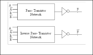
3.2 Complementary Pass-Transistor logic- (CPL)
CPL does not use pairs of two metal oxide semiconductor field effect transistors for the accomplishment of the low power logic functions. It utilizes only one type of MOSFETs that is N- type MOSFETs. This is the reason that by implementing CPL techniques, the circuits will have high operating speed. Also, the circuits need low value of input capacitance. CPL contains complementary inputs and outputs. It also includes an NMOS pass transistor logic network, and CMOS output inverters as shown in figure 1.
Fig.1. Basic Concept of CPL
As inverted and non-inverted inputs are needed to drive the gates of the pass-transistors, the complement of the logic also needs to exist which selects between the possible non-inverted output values which drives an inverter to generate an inverted version of the output [21].
The features of this logic style are increase in output node ca- pacitance, higher switching power dissipation and higher propagation delay [14]. The advantage of CPL is that design is modular. All gates use the same topology, only inputs are permuted. This makes design of a library of gates very simple. The availability of both polarities of every signal eliminates the need for extra inverters. Less number of transistors as PMOS transistors are eliminated [15], [16], [21], [22].The dis- advantage of CPL circuits is that the NMOS pass transistors have a threshold voltage drop. So CPL technique is not suita- ble for low supply voltages. Also one more disadvantage of this technique is that CPL based circuits are more sensitive to Voltage scaling than CSL CMOS [16].
3.3 Double Pass-transistor Logic- DPL
DPL is a modified version of CPL. The DPL also has compli- mentary inputs and outputs and thus it is implemented using dual-rails. In DPL circuits, full voltage swing is achieved at outputs by adding a PMOS transistor in parallel with NMOS transistors. Although the addition of PMOS transistors results in increased capacitance compared to CPL style but this does not limit the performance of DPL. DPL gates have balanced input capacitance, thus reducing the dependence of delay on input data. The problems of noise margin and speed degrada- tion in CPL circuits due to high reduced voltage level are solved out in DPL design style. The output buffers are not necessary, since the full swing is achieved by the addition of PMOS transistor.
The features of this logic style are low power consumption, complimentary inputs and outputs. Other advantage of DPL is that this technique eliminates the need for restoration circuit- ry. Also this technique has reduced delay as compared to the CPL and CSL techniques [17]. The disadvantage of DPL cir- cuits is the large area used due to the presence of PMOS tran- sistors of sizes doubles that of NMOS counterparts. The other drawback of this circuit is the required complementary inputs [18], [19], [20]
IJSER © 2014 http://www.ijser.org
International Journal of Scientific & Engineering Research, Volume 5, Issue 4, April-2014 860
ISSN 2229-5518
3.4 Gate-Diffusion Input - (GDI)
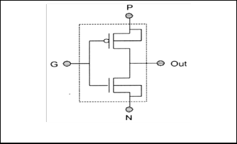
Gate diffusion input (GDI) - a new technology of low-power digital combinational designing of circuits - is presented in
2001[24]. GDI technology provides the designing of low power circuits and having low propagation delay. Also, this tech- nique results area efficient circuits due to the use of less com- plex logic designing. The different methods are compared with respect to the layout area, number of devices, de- lay, and power dissipation. The GDI method is based on the use of a simple cell as shown in Fig. 2. At first glance, the basic cell reminds one of the standard CMOS inverter, but there are some important differences.
1) The GDI cell contains three inputs: G (common gate input of NMOS and PMOS), P (input to the source/drain of PMOS), and N (input to the source/drain of NMOS).
TABLE 1
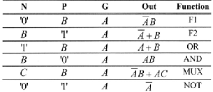
VARIOUS LOGIC FUNCTIONS OF GDI CELL FOR DIFFERENT INPUT CONFIGURATIONS [4].
2) Bulks of both NMOS and PMOS are connected to N or P (respectively), so it can be arbitrarily biased at contrast with a CMOS inverter.
It must be remarked that not all the functions are possible in standard p-well CMOS process but can be successfully im- plemented in twin-well CMOS or silicon on insulator (SOI) technologies [23]. In GDI based circuits huge variety of com- plicated logic functions can be accomplished with the use of few transistors. This method is suitable for design of fast, low- power circuits, using a reduced number of transistors (as compared to CMOS and existing PTL techniques). Table 1 shows how a simple change of the input configuration of the simple GDI cell corresponds to very different Boolean func- tions.
Fig. 2: Basic GDI cell.
Detailed in [4], GDI cell structure is different from the existing
PTL techniques. The features of this logic style are low power
consumption, improvements in design complexity level, tran-
sistor counts, static power dissipation and logic level swing.
Other advantage of GDI is that this technique reduces the transistor count. Also this technique has reduced delay as compared to the other PTL techniques [24].
4 POWER DISSIPATION AND ITS TYPES
The Power dissipation is the most critical parameter for porta- bility & mobility. It is classified in to Dynamic and Static pow- er dissipation. Dynamic power dissipation arises when the circuit is operational, while static power dissipation becomes an issue when the circuit is inactive or is in a power-down mode [26]. There are three major sources of power dissipation in digital CMOS circuits, which are summarized in (1) [18]:
Pavg = P switching + P short-circuit + P leakage
= (α0→1× CL×Vdd²×fclk) + (Isc × Vdd) + (leakage × Vdd)(1)
The first term represents the switching component of power, where load capacitance is CL; fclk is the clock frequency and α is the probability that a power consuming transition occurs (the activity factor). In second term direct-path short circuit current, Isc arises when both the NMOS and PMOS transistors are simultaneously active, conducting current directly from supply to ground. Finally, leakage current, which can arise from substrate injection and sub-threshold effects, is primarily determined by fabrication technology considerations [25].
The switching power dissipation is a strong function of the power supply voltage in CMOS digital ICs. Therefore, reduc- tion of emerges as a very effective means of limiting the power consumption. However, the saving in power dissipation comes at a significant cost in terms of increased circuit delay. Since the exact analysis of propagation delay is quite complex, a simple first order derivation [12] can be used to show the relation between power supply and delay time.
Td = CLVdd / K (Vdd - Vth) α (2)
K – Transistor‘s aspect ratio (W /L)
Vth- Transistor threshold voltage
α - Velocity saturation index which varies between 1 and 2
Unfortunately, reducing the supply voltage reduces power,
but when the supply voltage is near to threshold voltage (from
equation 2), the delay increases drastically [15].
4.1 Switching Power
It is consumed in charging and discharging of the circuit ca- pacitances during transistor switching.
4.2 Short-Circuit Power
IJSER © 2014 http://www.ijser.org
International Journal of Scientific & Engineering Research, Volume 5, Issue 4, April-2014 861
ISSN 2229-5518
It is consumed due to short-circuit current flowing from pow- er supply to ground during transistor switching. This power more dominates in Deep Sub Micron (DSM) technology.
TABLE2.
AND, OR, AND XOR CELLS USING GDI, CMOS, AND PTL DESIGN TECHNIQUES [4].
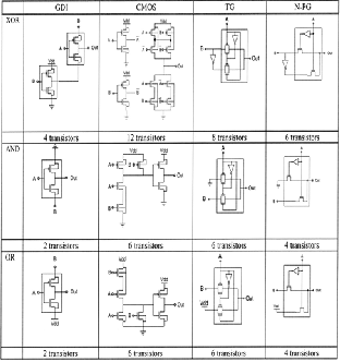
TABLE3.
COMPARISON OF VARIOUS DESIGNING TECHNIQUES
Features | CSL | CPL | DPL | GDI |
Transistor count | High | Low | Low | Very Low |
Delay | High | Very Low | Very High | Low |
Power Con- sumption | Very High | Low | High | Very Low |
• Jyoti gupta is currently pursuing her research work under the guidance of Mr. Amit Grover , Assistant Professor (ECE), Shaheed Bhagat Singh State Technical Campus, Ferozepur, Punjab, India. .
4.3 Static Power
It is consumed due to static and leakage currents flowing while the circuit is in a stable state. The first two components are referred to as dynamic power, since power is consumed dynamically while the circuit is changing states. Dynamic power accounts for the majority of the total power consump- tion in digital CMOS VLSI circuits at micron technology [19].
5 COMPARISON
Various techniques for digital circuit designing have been compared using table 2
Table 3 compares the different features of various digital de- signing techniques. Among all the design techniques, GDI proves to have the minimal number of transistors [4]. CSL technique consumes more power among all the techniques. CPL technique is also very efficient because it also consumes less power and produce lowest delay among all the designing techniques. GDI is the new approach for low power designing circuits because of its advantages. Only the CPL design style can be a better alternative for GDI if high-frequency operation is of concern [24].
6 CONCLUSION
All the circuits have been implemented on the basis of the re- quirement of different applications. Different logic styles have been proved to be efficient in various applications like most of the functions are complex in CMOS, as well as in standard PTL implementations, but very simple (only two transistors per function) in the GDI design method[14],[20]. In this paper we reviewed various digital designing techniques and dis- cussed various features, advantages and some drawbacks of them. Furthermore, we provide a comparison of some ele- ments of these techniques. However, more work and research is still going on to find out the other alternative techniques for the efficient designing of digital circuits.
REFERENCES
[1] M. Pedram, S. Nazarian, “Thermal Modeling, Analysis, and Management in
VLSI Circuits: Principles and Methods”, Proceedings of the IEEE, Vol. 94, No.
8, pp. 1487-1501, 2006
[2] E. S. Fetzer, M. Gibson, A. Klein, N. Calick, Z. Chengyu, E. Busta, and B. Mohammad, “A fully bypassed six-issue integer datapath and reg- ister file on the Itanium-2 microprocessor,” IEEE J. Solid-State Cir- cuits, vol. 37, no. 11, pp. 1433–1430, Nov. 2002.
[3] S. Naffziger, B. Stackhouse, T. Grutkowski, D. Josephson, J. Desai, E.
Alon, and M. Horowitz, “The implementation of a 2-core multi- threaded itanium family processor,” IEEE J. Solid-State Circuits, vol.
41, no. 1, pp. 197–209, Jan. 2006.
[4] A. Morgenshtein, A. Fish, I.A. Wagner, “Gate-Diffusion Input (GDI)
– A Power Efficient Method for Digital Combinational Circuits,” IEEE Trans. VLSI, vol.10, no.5 pp.566-581, October 2002.
IJSER © 2014 http://www.ijser.org
International Journal of Scientific & Engineering Research, Volume 5, Issue 4, April-2014 862
ISSN 2229-5518
[5] M. Golden, S. Arekapudi, G. Dabney, M. Haertel, S. Hale, L. Her- linger, Y. Kim, K. McGrath, V. Palisetti, and M. Singh, “A 2.6 GHz dualcore 64b x 86 microprocessor with DDR2 memory support,” in IEEE ISSCC Dig. Tech. Papers, Feb. 2006, pp. 104–105.
[6] A. M. Shams, T. K. Darwish and M. A. Bayoumi. “Permormance Analysis of Low Power 1-Bit CMOS full adder cells”, IEEE Transac- tion on VLSI Systems, Vol. 10, Feb. 2002.
[7] A. P. Chandrakasan, S. Sheng, and R. W. Brodersen, “Low-power
CMOS digital design,” IEEE J. Solid-State Circuits, vol. 27, pp. 473–
484, Apr. 1992.
[8] R. Zimmermann and W. Fichtner, “Low-power logic styles: CMOS versus pass-transistor logic,” IEEE J. Solid-State Circuits, vol. 32, pp.1079–1090, June 1997.
[9] K. Yano, Y. Sasaki, K. Rikino, and K. Seki., “Top-down pass- transistor logic design," IEEE J. Solid-State Circuits, vol. 31, no. 6, pp.
792-803,Jun. 1996.
[10] M. Anis, M. Allam, and M. Elmasry, "Impact of technology scaling on CMOS logic styles," IEEE Trans. Circuits and Systems II: Analog and Digital Signal Processing, vol. 49, no. 8, pp. 577-588, Aug. 2002.
[11] G. Merrett and B. M. Al-Hashimi, "Leakage power analysis and
comparison of deep submicron logic gates," in Proc. 14th Int.Workshop on Power, Timing, Modeling, Optimization, and Simu- lation (PATMOS),pp. 198-207, Sep. 2004.
[12] Bellaouar, A., and Elmasry, M. I., Low-Power Digital VLSI Design, Kluwer, Norwell, MA, 1995.
[13] D. Radhakrishanan, S.R. Whitaker, G.K. Maki, Formal design proce- dures for pass-transistor switching circuits, IEEE J. Solid-State Cir- cuits, 20(3): 531-536, 1985.
[14] L. Bisdounis, D. Gouvetas and O. Koufopavlou, “A comparative study of CMOS circuit design styles for low power high-speed VLSI circuits”, Int. J. of Electronics, Vol. 84, (6): 599-613, 1998.
[15] Sun, S., and Tsui, P., “Limitation of CMOS supply-voltage scaling by
MOSFET threshold voltage”, IEEE Journal of Solid-State Circuits, vol.
30, pp. 947-949, 1995.
[16] D. Radhakrishanan, Low-voltage low-power CMOS full adder,in
Proc. IEE Circuits Devices Syst., vol. 148, Feb. 2001.
[17] Issam S. Abu-Khatter, Abdellatif bellaouar, and M.I. Elmasry, Circuit Techniques for CMOS Low-Power High-Performance Multipliers, IEEE J. Solid- State Circuits,31(10): 1535-1546,1996.
[18] Weste, N., and Eshragian, K., Principles of CMOS VLSI Design: A Systems Perspective, Pearson Addison-Wesley Publishers, 2005.
[19] S. Devadas and S. Malik, A survey of optimization techniques target- ing low power VLSI circuits, in Proc. 32nd ACM/IEEE Design Au- tomation Conf., pp. 242–247, 1995
[20] A. P. Chandrakasan and R. W. Brodersen, “Minimizing power con- sumption in digital CMOS circuits,” Proc. IEEE, vol. 83, pp. 498–523, Apr.1995.
[21] W. Al-Assadi, A. P. Jayasumana, and Y. K. Malaiya, “Pass-transistor logic design,” Int. J. Electron., vol. 70, pp. 739–749, 1991.
[22] A. Chandrakasan, W. J. Bowhill, and F. Fox, Design of High Perfor- mance Microprocessor Circuits, 2000, ch. 5, pp. 80–97.
[23] K. Bernstein, L. M. Carrig, C. M. Durham, and P. A. Hansen, High
Speed CMOS Design Styles. Norwell, MA: Kluwer Academic, 1998. [24] “Gate-diffusion input (GDI)—A novel power efficient method for
digital circuits: A design methodology,” presented at the 14th Int. ASIC/SOC Conf., Washington, DC, Sept. 2001.
[25] D. Wang, M. Yang, W. Cheng, X. Guan, Z. Zhu, Y. Yang Novel Low
Power Full Adder Cells in 180nm CMOS Technology Industrial Elec- tronics and Applications, pp 430-433, 2009.
[26] P. C. H. Meier, Analysis and Design of Low Power Digital Multipli- ers, Ph.D. Thesis, Carnegie Mellon University, Dept. of Electrical and Computer Engineering, Pittsburgh, Pennsylvania, 1999.
AUTHOR’S BIOGRAPHY


Jyoti Gupta received her B. Tech degree in Electronics and Communication Engineering in 2012 from Baba Farid College of Engineering and Technology, Affiliated to Punjab Technical University, Kapurthala, Punjab, India. Her place of birth is Ferozepur, Punjab, India on 20th April, 1990. At present she has been doing her research work under the guidance of Mr. Amit Grover, Assistant Professor, Department of ECE, Sha- heed Bhagat Singh State Technical Campus, Moga road, Ferozepur-152004, Punjab, India.
Amit Grover (M’06-SM’09-PI’11&12) The author became a Member (M) of Association ISTE in 2006, a Senior Member (SM) of society SELCOME in September 2009, and a Project-In charge (PI) in august 2011 and in September 2012. The author place of birth is Ferozepur, Punjab, India on 27th, September
1980.The author received his M. Tech degree in Electronics and Communication Engineering from Punjab Technical Uni- versity, Kapurthla, Punjab, India in 2008 and received his B. Tech degree in Electronics and Communication Engineering from Punjab Technical University, Kapurthala, Punjab, India in 2001. Currently, he is working as an Assistant Professor in Shaheed Bhagat Singh State Technical Campus, Ferozepur, Punjab, India. The author is a Reviewer of many International Journals. His area of interest includes signal processing, MIMO systems, Wireless mobile communication, High speed digital communications and 4G Wireless Communications.
IJSER © 2014 http://www.ijser.org