(AES) was published by NIST (National Institute of Standards and Technology) in 2001[6]. The Rijndael algorithm has four main operations. They are
International Journal of Scientific & Engineering Research, Volume 4, Issue 4, April-2013 1143
ISSN 2229-5518
FPGA Based SCA Resistant AES S-Box Design
S.Sankar Ganesh1, J.Jean Jenifer Nesam2
2.6 Mega Byte that optimizes the chip area and composite field S-box reduces the power consumption and masking module used to increase the system security.
I. INTRODUCTION
In today’s world information sharing between computer and communication network need a high security standard. The AES is strong security standard that become effective on May 26, 2002 by NIST to replace DES. The DES algorithm broken because of its short keys(56-bit key). The AES uses 128 bit input and the key length is 128 bit, 192 bit or 256 bits. AES can be implemented easily on software.
Important thing in improved AES is the design of S-box uses masking module. In this paper introduce mask able values for S-box, which means the value that has to be substituted is masked by Masking module. Thus the original S-box values are masked for secured transmission of information. This proposed masking module can be implemented on any part of the AES algorithm. This module works under power saving mode. When the module is enabled then only it consumes power otherwise it in off mode.
The LOOK-UP TABLE based (LUT) S-box design consumes more than 75% power of overall architecture. Thus the mode of operation of S-box based on LUT is replaced by composite field in this project.
II. ADVANCED EENCRYPTION STANDARD (AES) -128
1. Brief Explanation of Rijndael Algorithm
The Rijndael as Advanced Encryption Standard
(AES) was published by NIST (National Institute of Standards and Technology) in 2001[6]. The Rijndael algorithm has four main operations. They are![]()
1.S.Sankar Ganesh, Asst.Professor,School of Electronics Engineering,VIT University,Vellore,Tamil Nadu. Email:s.sankarganesh@vit.ac.in
2.J.Jean Jenifer Nesam
Email:jeanjenifer@rediffmail.com
a) Byte substitution (sub bytes)
b) The shiftrows c) Mixcolumns
d) Round key adding(Add round key)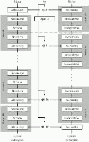
Fig.1. AES Encryption and Decryption
AES-128 encryption consists of 10 rounds of transmission of the input plaintext for the cipher text. For AES-128 bit the corresponding key length is 128 bits[6]. In this paper only AES-128 encryption scheme with 128 bit key is considered. Byte substitution is the non linearity function. This includes the byte substitution from the Rijndael S-box. Shift rows operation performed on each state in state matrix. In AES 1st row is unchanged and other rows are shift their position according to their row numbers.
During the mix column operation each column is multiplied with known matrix and multiplication
International Journal of Scientific & Engineering Research, Volume 4, Issue 4, April-2013 1144
ISSN 2229-5518
performed in different manner. Round transmission is the simple xor function performed on round key and
mixcolumn output[3].
2. Two main process of AES-128:
The new improved AES algorithm consists of two
main operations a) key schedule and b) round
transformation.
Key schedule has two operations:
Key expansion and round key selection. Key expansion means expand the input key based on some operations and round key selection means select the Nb bits from the expanded key.
Round Transformation involves four modules
by subbyte, shiftrows, mixcolumn and Add Round key.
III.POWER ANALYIS OF S-BOX:
Power analysis of the s-box is based on timing simulation. It gives quite accurate estimation compared with static analysis.By investigating the power consumption of each primitive component in AES circuits, we found the LUT based S-Box in the SubBytes component consumes much of the total (for instance, 75% is consumed in a 1 round/cycle loop architecture).
Our paper proves the dynamic power reduction in our composite field AES S-box. It is also a simple but an effective measure to reduce dynamic hazards in the circuits with complicated signal paths, such as composite field AES S-box. But the composite field operation increases the dynamic hazard.
IV. THE LOW POWER S-BOX DESIGN
The S-box implementation is the complicated process in the AES architecture. The S-box can be designed on the ROM where the S-box values are stored. This is known as Look-Up Table (LUT) s-box.
It means that the operation based on LUT needs a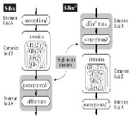
memory (256x8 bit=1024 bit). Thus the S-box memory consumes 75% of the power of overall AES architecture[7]. To improve the operation of S-box firstly, need low power consumption. This can be achieved by using composite field S-box design.
Fig.2. Composite field operation
The composite field S-box design reduces the power consumption to acceptable level. The S-box based on composite field uses Galois field GF(22)2)2) format that uses less number of gate circuits[9]. The composite field uses less number of gate count may reduce the area of architecture. Complexity of this composite field S-box is heavily dependent on three factors: i.e. the field of mapping, the representations of the field elements (the field polynomials and basis representations used), and the isomorphic mapping chosen for representation. Thus, one can conveniently take advantage of the isomorphism to map a computation from one field to another in the search for the most efficient implementation. In this work, we employed a composite field AES Sbox that strikes a balance between minimal circuitry area and short critical path.
V. SIDE CHANNEL ATTACKS
A side-channel is any observable information emitted as a byproduct of the physical implementation of the cryptosystem. Possible Side Channels are Power, Time, Faults Electro-Magnetic radiations, Sound , Scan Chains and may many more..
Timing AttacksWorks by correlating timings of a target machine to those of an identical reference machine with a known key.
Power Analysis AttackAnalysis the power of the circuit with the reference machine able to find the key.
VI. MASKING S-BOX VALUES
In AES algorithm, the substitute byte function uses
S-box values. The S-box is like a matrix form ROM memory which has a fixed value within it. If we observe the power from ROM, there is a possibility to find the S-box value that may leak the message content[4]. The power is easily observed from ROM memory by adding small value of resister in parallel with Rom and observing voltage drop across it, gives the power of ROM memory.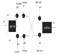
Fig.3. Masking operation
International Journal of Scientific & Engineering Research, Volume 4, Issue 4, April-2013 1145
ISSN 2229-5518
By masking S-box value, if we analysis the power also does not give the original value. By reversing the operation in next step in AES algorithm we can retrieve the original S-box value. The above diagram shows how the masking function is implemented. The output of S-box is 8 bit. By doing some internal operation we can convert 8 bit S-box value into another one value.
VII. MASKING MODULE
The splitter is used for splitting the 8 bit input from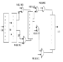
S-box to two 4 bit sequences.
Fig.4. Masking module
This 4 bit sequences then expanded to 128 bit by
using expander module. Two different internally generated
128 bit PN sequence is “XOR”ed with expanded 128 bit output independently. The next step the sequences are again “XOR”ed with two different 12 bit fixed values. The fixed values are written by the programmer in the coding itself we cannot change that value from externally. The swapping operation is then performed. Now the original masking value of input shuffled with other bits. Finally, from the the 128 bit each output the needed outputs are combined together to form an 8 bit output.
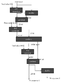
1. PN Sequence Generation
The user can enter any combination of 8 bit string of 0’s
and 1’s. The module stores 8 bit value which can be
“AND” ed with 8 bit input.
Fig.5.PN sequence generation
The resultant output is given to shuffler that gives
another 8 bit which is differ from AND operation output. Then both outputs are combined together and form a 16 bit output. This type of shuffling and combining are performed until the 128 bit PN sequence is generated. Thus the 8 bit input is converted to 128 bit then “xor”ed with the expander output. PN generation depends on one output as another one input ie, it may be run as a sequential module which causes some delay in the output.
VIII. DE-MASKING MODULE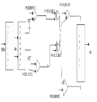
Fig.6. De-masking module
By reversing the masking module we can retrieve the original data. De-masking also need the same resources thus we can share the resources of masking module.
IX.FUNCTIONAL SIMULATION RESULTS
The algorithm proposed in this paper is then implemented by using VHDL description language.
International Journal of Scientific & Engineering Research, Volume 4, Issue 4, April-2013 1146
ISSN 2229-5518
1.Simulation using modelsim ALTERA 6.6c platform:
All files are complied by using modelsim ALTERA
6.6c and then the waveforms are obtained from wave block.
Fig 7.masked s-box output
The s-box values are given as byte_in which is a 8
bit input it produces a output same as look up table value. Then the value is masked with masking module produces a new masked value.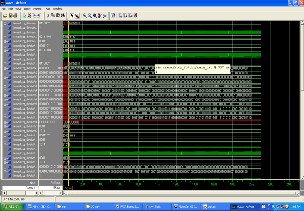
Fig.8 Re-masked s-box output
Re-masking removes the mask to give us the
original s-box value.
2. Synthesis result of AES s-box using Xilinx ISE 9.2i:
The design of AES using reduced power S-Box is done using VHDL and implemented in Xilinx Virtex-5
XC5VLX50 (package: Spartan3e 2s50eft256, speed grade: -6)
FPGA using the ISE 9.2i design tool. Table2, table 3 shows the FPGA implementation results of AES using reduced power composite field based S-Box.
It describes the selected target Xilinx spartan device, encryption throughput achieved, timing reports and the overall device utilization. Synthesis result of the masked s-box is given below in figure.8
Fig.9. Synthesis result of masked s-box.
Synthesis result of re-masked s-box design is given in the
below figure 10.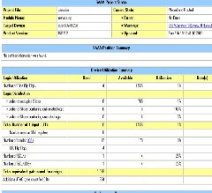
Fig.10.Synthesis result of Re-Masked s-box
The synthesis result shows that the design is fit successfully with the specific pins. The summary of composite field s-box can be extracted from the design summary option. Then the comparison can take place. The composite field s-box gives the better performance.
The s-box design can be fit successfully in CPLD
family device also. The fitting summary of s-box design is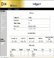
given below
International Journal of Scientific & Engineering Research, Volume 4, Issue 4, April-2013 1147
ISSN 2229-5518
Fig.11. CPLD summary
3.Design summary:
The design summary comparison of the LUT base s-box and composite field s-box is given below
Table.1. comparison of LUT and composite field s-box.
The synthesis & mapping results of masking s-box are summarized in Table2.
Table.2. Implementation results of masked s-box
SelecDteedsiDgnevice
STpoatratal nm2eemory
2s50eft256-6
: LUT s-box 145772
45 out of
Number of
Slices: Composite
umber of
kilobytes
768 5%
119788
8 out of
N field s-box
kilobytes
Slice Flip Flops:
Number of 4 input LUTs:
Number used as logic: Number used as Shift registers Number of IOs:
Number of bonded IOBs Number of GCLKs
1536 0%
84 out of
1536 5%
76
8
26
18 out of
178 10%
1 out of 4
25%
The design summary of composite field s-box is given above. Thus the summary comparison shows that
Clock period 3.792ns
max frequency 263.713MHz
composite field s-box can reduce the memory by reducing the cell usage. Thus the composite field s-box can save the
Total memory usage
136328 kilobytes
area up to 2.6 Mbytes[8].
X. CONCLUSION
The synthesis & mapping results of re-masking s-box are summarized in Table3.
Table.3. Implementation results of re-masked s-box
The implementation of FPGA Based SCA Resistant AES S- Box Design is proposed in this paper. After being coded with VHDL, the waveform simulation of the new AES algorithm was taken in modelsim altera 6.6c platform. Composite field s-box reduces the chip area. The power consumption is directly connected with chip area.
Therefore the results reduce the power
consumption. Implementation of masked s-box increases
the system security and hence increases the algorithm’s
performance. The composite field s-box design uses a less
International Journal of Scientific & Engineering Research, Volume 4, Issue 4, April-2013 1148
ISSN 2229-5518
number of gates that reduces the chip area. Composite field s-box creates dynamic hazards. The future research could be a reduction of those dynamic hazards and also reduction of delay due to sequential order of PN generation.
REFERENCES
[1] AI-wen luo, Qing-Ming Yi, Min Shi “design and
implementation of area optimized AES BASE on FPGA”,
IEEE Inter.conf.chal sci com Engin., 978-1-61284-109-0/11.
[2] Ahmed Rady,Ehab EL Sehely,A.M. EL Hennawy “Design and Implementation of area optimized AES algorithm on reconfigurable FPGA”IEEE Inter.Conf. Comp ElecEngin.(IECEE), 978-1-4244-1847-3/07.2007.
[3]Federal Information Processing Standards Publication
197 November 26,2001“ADVANCED ENCRYPTION
STANDARD (AES)”.2001
[4]Francesco Regazzoni1,3, Yi Wang2, Franc¸ois-Xavier
Standaert1the “FPGA Implementations of the AES Masked
Against Power Analysis Attacks”
[5] J.Yang, J.Ding, N.Li and Y.X.Guo,“FPGA-based design and implementation of reduced AES algorithm” IEEE Inter.Conf. Chal Envir Sci Com Engin(CESCE).,Vol.02, Issue.5-6, pp.67-70, Jun 2010.
[6] NIST, “Advanced Encryption Standard (AES)”, NIST,
FIPS-197, 2001.
[7] M. M. Wong and M. L. D. Wong Swinburne University
of Technology (Sarawak Campus),Jalan Simpang Tiga,
93350, Kuching Malaysia.“A High Throughput Low Power Compact AES S-box Implementation using Composite Field Arithmetic and Algebraic Normal Form Representation”
978-1-4244-7808-8/10 ©2010 IEEE
[8]M.R.M. Rizk, Senior Member, IEEE and M. Morsy
“Optimized Area and Optimized Speed Hardware
Implementations of AES on FPGA”.2007.
[9] Rizk.M.R.M. and Morsy, M.,“Optimized Area and Optimized Speed Hardware Implementations of AES on FPGA”, IEEE Inter Conf. DesigTes Wor.,vol.1,issue.16,pp.207-217, Dec. 2007.
[10] Satoh. A , Morioka. S , Takano. K , and Munetoh .S, “A Compact Rijndael Hardware Architecture with S-Box Optimization”,LNCS2248, ASIACRYPT 2001, pp.239-254,
2001. 256.
International Journal of Scientific & Engineering Research, Volume 4, Issue 4, April-2013
ISSN 2229-5518
1149