
International Journal of Scientific & Engineering Research, Volume 6, Issue 5, May-2015 347
ISSN 2229-5518
Author : M.S.Koushik
Abstract-Human skin is an important organ. It consists of an integrated, stretchable network of sensors that relay information about tactile and thermal stimuli to the brain, allowing us to move the organs within our environment safely and effectively. inspired by human skin an ELECTRONIC SKIN is created by artificial means used for autonomous intelligent robots and biometric prosthetics, among other applications. The development of electronic networks comprised of flexible, stretchable, and robust devices that are compatible with large-area implementation and integrated with multiple functionalities is a testament to the progress in developing an electronic skin (e-skin) to human skin. E-skins are already capable of providing augmented performance over their organic counterpart, both in superior spatial resolution and thermal sensitivity. They could be further improved through the incorporation of additional functionalities (e.g., chemical and biological sensing) and desired properties (e.g., biodegradability and self-powering).Continued rapid progress in this area is promising for the development of a fully integrated e-skin in the near future.
Keywords-,Artificial Skin, Biometric Prostheses ,Electronic Skin, MEMS Technology, Optoelectronics, Robotics, Self-Healing, Sensitive Skin, Super capacitors.
1 INTRODUCTION
—————————— ——————————
Human skin is highly intuitive, making it easy to neglect the complexity of the largest sensory organ in our body, SKIN. Our skin is the physical barrier through which we interact with our surroundings. It allows us to perceive various shapes and textures, changes in temperature, and varying degrees of contact pressure. To achieve such high sophistication in its sensing capabilities, several different types of highly specialized sense receptors are embedded within our skin. These receptors first transducer information generated by physical contact into electrical signals and subsequently send it to the central nervous systems for more complex processing. The collected signals are eventually interpreted by the somatosensory cortex, permitting us to successfully navigate our physical world with ease. The effort to create an artificial skin with human-like sensory capabilities is motivated by the possibility of such large, multi- sensory surfaces being highly applicable for autonomous artificial intelligence (e.g., robots), medical diagnostics, and replacement prosthetic devices capable of providing the same, if not better, level of sensory perception than the organic equivalent. Endowing robots with sensing capabilities could extend their range of applications to include highly interactive tasks, such as caring for the elderly, and sensor skins applied on or in the body could provide an unprecedented level of diagnostic and monitoring capabilities. An artificial skin with such sensory capabilities is called as sensitive skin, smart skin, or electronic skin (e-skin).
IJSER © 2015 http://www.ijser.org
International Journal of Scientific & Engineering Research, Volume 6, Issue 5, May-2015
ISSN 2229-5518
348
.·......................................................................................................
1970
BI·On·iC "SI'X MI'llI'On 00IIar Man"141 ;
Prosthetic hand in Star Wars 5
lnfrar d
181
e-skm
[12)
1991
61
Robot in Terminato,J
'
'•---------------------------------------------------
[334a)
Organic transistor e-nose
Sensitive Skin Workshop
1111
1999
. k' . [12) - - ----..---,
1rs e-s 1n v1ew
Large-scale organ1.c c1.rcu1'ts....--2000
2(i)01
[157a]
Stretchable inverters
Flexible, 2004
High-rs optical 12401
tact1le sensor
Anthropomorphic, 14251
bernetic hand
activ - . 1266a]
matnx e-sk1n
2006
[267)
2007 -........_Wireless electronics
2008
Micro-structured pressure sensor
20 9 -........_Stretchable OLEOs
2010 radable OFETs
[20b]
-lJnc
1181
13761
[21a)
Stretchable OPVs
Epider al 1389a]
electronics
2 11
Ultrafl xi le .
11191
Intrinsically stretchable a]
120
OLEOs
Stretchable,
C CirCUitS
Macro cale . [?2a]
nanow1re e-sk1n
01 [19]
transparent
1471
e-skin
Self-healing e-skin
[258]
Stretchable,11461
buckled transistors
Interlocked e-skin
. [377)


Rechargable,
11341
stretchable batteries
Bioresorbable Si circu1ts
Ultrathin b]
121
stretchable OPVs
International Journal of Scientific & Engineering Research, Volume 6, Issue 5, May-2015 349
ISSN 2229-5518
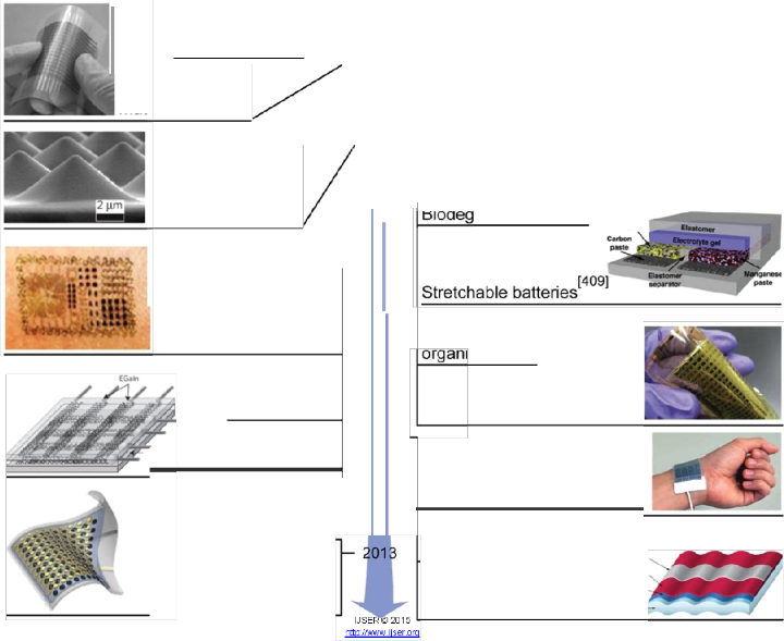
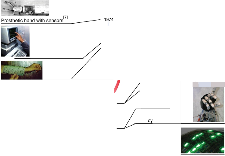
Figure : A brief chronology of the evolution of e-skin.several science fictional events in popular culture that inspired subsequent critical technological advancements in the development of e-skin are emphasized: ―micro-structured
pressure sensor‖,
―stretchable O LED s‖ , ―stretchable O PV s‖, ―stretchable, transparent e-skin‖ , ―m acroscale
nanowire e-skin‖, ―rechargeable, stretchable batteries‖, ―interlocked e-skin.‖ C opyright, respectively, 2010, 2009,
2012, 2005, 2010, 2013, 2012. Macmillan Publishers Ltd. ―Flexible, activematrix e-skin
2 ARCHITECTURE
Electronic skins for robots and medical prostheses—multifunctional structures, in which sensors and actuators are closely integrated with microelectronic circuits—bring a new dimension to electronics flexibility. Shaped electronics and skin-like electronics may experience large deformation strains. A disk detector array may see its surface area double to be shaped as a hemispherical detector array. When wrapped over elbow like joints, the skin may be stretched and relaxed many times by 15%. Semiconductor integrated circuits and MEMS technology use rigid and stiff substrates that are not adapted to flexible structures, and thin active device materials that fracture at a critical strain of
1% .Free-standing thin metal films also break under tensile strain of the order of 1%.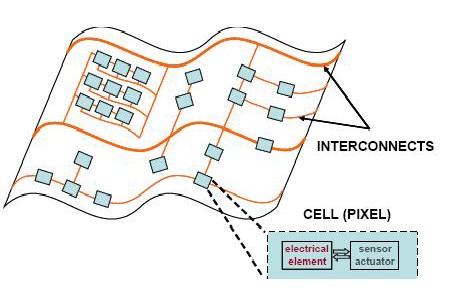
Figure: island carrying electronic surface
To achieve flexible and stretchable skin, sub circuit cells, made of a transducer and an electronic circuit, will be placed on mechanically separated islands, which are fabricated on a deformable substrate that takes up most of the total strain. The figure shown above is a sketch of such an island carrying electronic surface. The islands are made sufficiently rigid to protect them from breaking when the circuit is deformed one time or by repeated stretching. The sub circuits are electrically connected with stretchable metal conductors.
We have three options for making deformable interconnects: making thin metal films that can withstand large plastic deformation, deforming a sacrificial mask which serves in liftoff metallization, and making stretchable metallization.
IJSER © 2015 http://www.ijser.org
International Journal of Scientific & Engineering Research, Volume 6, Issue 5, May-2015 350
ISSN 2229-5518
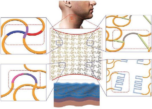
Figure : Detailed view of inner circuit of electronic skin
3 FEATURES
The electronic skin concept was initially developed for applications in robotics.Robots could be provided with pressure sensing (―touch‖)thatw ould alow them to grip objects securely w ithout damaging them (the ―picking up an egg‖ problem ). T hese electronic skins, w hich m ainly consist of pressure - sensing materials and associated
electronic devices for pressure reading, might also provide touch sense to prosthetic devices such as artificial legs or arms. One challenge for making these devices is that the transistors (and the semiconductors in them) that amplify weak signals must be flexible in order to act like skin. The ability of transistors to amplify signals, their gain depends on the mobility of the charge carriers in their semiconductor under the gate layer (or in their gated semiconductor layer). Doped single-crystalline silicon wafers are used in most computer chips because of their high carrier mobility, which allows operation with low applied voltage and low power. However, the wafers are brittle, so alternative materials have been pursued. Some of the candidate flexible semiconductors, such as conducting polymers have much lower carrier mobility.The higher voltages needed to use these materials as transistors may not be suitable for electronic skin that makes direct contact with a patient’s skin, and may quickly exhaust small power supplies. Another approach is to convert brittle semiconductors into more flexible forms. For example, silicon and germanium are highly flexible as nano wires. However, their carrier mobility, although much higher than that of conducting polymers, is still much lower than that of doped silicon. With these types of materials, it is difficult or impossible to achieve the performance needed to amplify very weak signals acquired from natural skin.
IJSER © 2015 http://www.ijser.org
International Journal of Scientific & Engineering Research, Volume 6, Issue 5, May-2015 351
ISSN 2229-5518
The electronic skin uses thin single-crystal silicon that has superior flexibility and a mobility equivalent to that of the silicon used in personal portable devices. The approach, a printing method developed previously by
Rogers’s group could be called ―inking and printing. ‖
A thin silicon layer is bonded to a silicon dioxide release layer. The silicon layer is cut into a lattice of micrometer-scale ―chiplets,‖ and a transfer stam p layer is then attached to the top of the divided
silicon. The transfer layer and chiplets are then lifted and transferred to a flexible substrate. Attaching electronic skin to natural skin is more difficult than attaching it to robots or prosthetics. Natural skin is soft and delicate and already has touch-sensing functions. The electronic skin that can be used for physiological monitoring must have a supporting layer with mechanical properties that match those of natural skin to avoid any discomfort resulting from long wearing. The electronic skin must not be too thick, too rigid, too hard, or too heavy, but must have conformal contact, intimate integration, and adequate adhesion with the natural skin. Special materials that are properly designed through accurate modeling were needed to achieve these properties. The support layer of the electronic skin is an elastomeric (rubbery) polyester engineered to have mechanical properties well matched to those of natural skin. The circuitry part of the electronic skin consists of two protection layers that sandwich a multifunctional middle layer. With their equal thicknesses, the protection layers develop opposite strains that cancel, so the middle circuit layer experiences little stress no matter which direction the device is bent. The middle layer consists of the metal, semiconductor, and insulator components needed for sensors, electronics, power supplies, and light-emitting components, all of which are in the serpentine shape that forms a stretchable net. The serpentine shapes allow the net to deform drastically with little effect on its functionality.
This innovative design contains all of the necessary components in an ultrathin layer about the
thickness of a human hair. The electronic skin can be simply mounted onto or peeled off natural skin in the same way
as bandage tape. Physiological information has been collected from heart, brain, and skeletal muscles with a quality
equivalent to that collected with bulky electrodes and hardware. Other forms of physiological information collection
based on the electronic skin are readily feasible because they could use components that have more sophisticated functions. The transfer-printing fabrication approach has proved to be viable and low-cost in this demonstration, which will greatly facilitate the practical clinical use of the electronic skin. Because of the higher quality of the transferable thin silicon, wireless communication directly from the electronic skin should be feasible, given recent demonstrations of this capability in other devices .Other types of electronic skins with applications beyond physiology, such as body heat harvesting and wearable radios, may also point to interesting directions for future work.
4 DESIRABLE PROPERTIES FOR E-SKIN
E-skin can mimic the properties of human skin in its ability to sense tactile forces, as well as augment the capabilities of human skin through incorporation of chemical and biological sensing functionalities.
Biocompatibility and Biodegradability
Since e-skin applications require intimate association with biological interfaces, biocompatibility is an important consideration for such devices. Ideally, e-skin should be synthesized from highly biocompatible components.
Self -healing
While naturally occurring human skin has the ability to repair itself after incurring mechanical damage, this property has yet to be fully realized in e-skin. For artificial skin, the ability to repair both mechanical and electrical damage would be highly advantageous for practical applications. There are two predominant strategies used to incorporate self-healing properties into materials, namely: 1) the use of materials loaded with healing agents and 2) the use of materials containing dynamic reversible bonds. The incorporation of capsules containing healants was first demonstrated in self-healing, non-conducting polymers. However, for e-skin applications, it is necessary to use a system that is electrically active.
Temperature sensitivity
IJSER © 2015 http://www.ijser.org
International Journal of Scientific & Engineering Research, Volume 6, Issue 5, May-2015 352
ISSN 2229-5518
Sensing temperature is a key functionality of human skin that helps to prevent injury and provides information about the surrounding environment, most tactile sensors are inherently temperature sensitive, and their response must therefore be calibrated with a temperature sensor. Several groups have implemented piezoelectric pyroelectric sensors that can discriminate between temperature and pressure inputs. Resistive temperature detectors (RTD) are attractive for e-skin applications owing to their flexibility, simple device structure, and compatibility with electronic readout methods.
RTDs relate a change in temperature to a corresponding resistance change through a material commonly composed of metals such as Au and platinum (Pt). To deconvolute the contribution of tactile stimuli from temperature sensors, meandering sections of Pt as temperature-sensing devices were implemented . These devices achieved a resolution of 0.03 °C over a wide range of temperatures. stretchable temperature sensors based on thin, buckled Au lines are also demonstrated .While the linear behavior of this sensor was attractive, the change in resistance was relatively small, and would require a sensitive readout mechanism.
Self – Powering
Providing a long-lasting supply of power is a persistent challenge for mobile electronics. As the largest human organ, skin provides a large area for potential energy storage. Furthermore, as the body’s interface with the outside world, e-skins may provide the opportunity to scavenge energy from environmental sources such as light and mechanical forces. A number of promising technologies have recently been demonstrated for power generation, transmission, and storage in stretchable systems, including solar cells, mechanical energy harvesters, supercapacitors, batteries, and wireless antennas.
Light is a readily available power source, and is most effectively harvested using devices with large surface area. stretchable solar cells based on rigid GaAs device islands connected with freestanding metal interconnects are determined . These solar cells operated with an efficiency of ≈13% with applied strain of up to 20%. Although these devices provided exceptional performance, the high cost of GaAs may limit its implementation in large-area e-skins. OPVs on ultrathin substrates using conventional materials and processes are fabricated . By transferring the devices to a prestretched substrate, they were able to achieve a stretchability up to 400% with an efficiency of 4%.
Technologies for harnessing mechanical energy include both dielectric elastomer generators and piezoelectric generators. Dielectric elastomer generators consist of an elastomeric dielectric coated with two highly compliant electrodes, and their stretchability makes them attractive for use in e-skin. The electrodes are charged by applying a voltage in the compressed state. Relaxation of the elastomer increases the voltage, producing higher energy charges that are harvested. Dielectric elastomer generators can achieve very high efficiencies, but have historically been limited by the complexity and weight of the associated electronics. Recent reports have demonstrated that the circuit complexity can be reduced using systems that are self-primed or primed by electrets. Mechanical energy harvesting devices based on nanostructured piezoelectric materials have also been developed, and stretchable versions have been fabricated by buckling the active materials. Fueled by the development of new soft materials, the field of mechanically compliant energy storage technologies has recently emerged.
Supercapacitors store energy in the form ofdouble layers of charged species residing at the electrode– electrolyte interface and provide very high power densities. Buckled CNT electrodes on prestrained substrates have been used to make supercapacitors that are stretchable up to 30%.
IJSER © 2015 http://www.ijser.org
International Journal of Scientific & Engineering Research, Volume 6, Issue 5, May-2015 353
ISSN 2229-5518
5 HIGHLY INTEGRATED ELECTRONIC SKIN DEVICES
Using the technologies described in previous sections, highly integrated systems of mechanically compliant sensor arrays possessing multiple functionalities have been reported. A select number of recent advancements will be described in this section, along with some of their demonstrated applications in the fields of biomedical devices, robotics, and optoelectronics.
Biomedical Devices
Active electrode arrays have been demonstrated for measuring electrical activity in both the heart and brain. The mechanical compliance of these arrays was essential for achieving conformal interactions with these irregularly shaped organs. For measuring electrocardiogram signals, an array of 2016 transistors was used to achieve good temporal resolution at 288 contact points, thus allowing for high-resolution spatial mapping of electrical characteristics. A similar flexible array of active electrodes was used to measure brain activity with unprecedented spatial accuracy.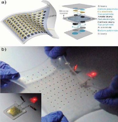
Figure: Demonstration of stretchable lithium ion batteries.
a) Illustration of a stretchable device with an exploded view of the various layers in the battery structure.
b) Operation of a battery that has been biaxially stretched to 300% powering a red LED. Inset shows the un stretched device
IJSER © 2015 http://www.ijser.org
International Journal of Scientific & Engineering Research, Volume 6, Issue 5, May-2015 354
ISSN 2229-5518
Robotics
Compliant devices with integrated tactile functionality could be used as skin-like sensors for intelligent robots. One of the first flexible and highly multifunctional skin-like systems was reported using polymer micromachining technologies. An array of several sensor types allowed the measurement of numerous desired parameters such as contact forces, object hardness, temperature, thermal conductivity, and surface curvature. However, the system lacked multiplexing for large-scale implementation.
Over the last decade, a series of increasingly more complex stretchable circuits with multiple functionalities were reported. A flexible active matrix of pressure and temperature sensors was first reported in 2004,and stretchability was subsequently added by the selective removal of periodic sections of the flexible substrate. To increase the device’s stretchability, stretchable interconnects were implemented by developing a highly conductive and stretchable material comprised of a fluorinated elastomer and ionic liquid with long CNTs. The stretchable material was later formulated to be printable, thus improving the throughput and cost effectiveness of the device’s manufacturing process.
The adopted active matrix technology has subsequently been used to drive a range of devices, including pressure sensors, temperature sensors, electromagnetic interference sensors, and actuators for tactile feedback arrays. By integrating a floating gate into their OFETs, pixels with memory capabilities were created that could locally store information from piezoresistive elements. For device readout, local memory is important to capture transient events
that may be shorter than the readout time of the sensor array and to provide a ―snapsho‖t
distribution of the stimulus.
Optoelectronics
of an instantaneous
Stretchable optoelectronics for applications such as stretchable or semitransparent displays, biomedical imaging, and hemispherical photodetector (PD) arrays are promising. Traditional planar PD arrays require complicated optics and/or image correction software to extract an accurate image. Curved PDs similar to the human retina have been developed that can simplify the required optics, reducing the cost and weight of the detector. Furthermore, detectors with adjustable forms can provide dynamically tunable zoom and focusing and can mimic the sophisticated imaging system of insect eyes.
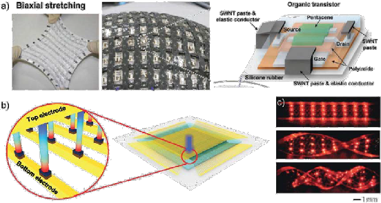
Figure : Highly integrated e-skins for robotics and optoelectronic applications
IJSER © 2015 http://www.ijser.org
International Journal of Scientific & Engineering Research, Volume 6, Issue 5, May-2015 355
ISSN 2229-5518
a) Stretchable active matrix devices including biaxial stretching of an integrated, encapsulated device demonstrating a conformal coverage of a non-planar surface (left), and a depiction of an individual organic transistor in the array (right).
b) Depiction of piezoelectric NWs used as an array of active tactile sensors with unprecedented spatial density.
6 CONCLUSIONS
In the past decade, the pace of e-skin development has accelerated dramatically owing to the availability of new materials and processes. As a result of this progress, the capabilities of e-skin are rapidly converging.
Interest in e-skin has been driven by its potential to:
1. enable highly the development of interactive and versatile robots that are capable of performing complex tasks in less structured environments.
2. facilitate conformable displays and optics. and
3. revolutionize healthcare by providing biometric prostheses, constant health monitoring technologies, and
unprecedented diagnostic and treatment proficiency.
Sensors and circuits have already exceeded the properties of biological skin in many respects. Electronic devices have been fabricated that stretch many times further than skin, flexible tactile sensors have been demonstrated that possess vastly superior spatial resolution to human skin, and tactile and temperature sensors are available with enhanced sensitivity over their natural counterpart.
Despite rapid progress, there is a continuing need for further development before the goal of integrating multiple functionalities into large-area, low-cost sensor arrays is realized. From a design standpoint, e-skin requires active circuitry to address large numbers of devices with minimal wiring complexity and fast scan rates. Furthermore, the ability to mimic the mechanical properties of human skin (e.g., flexibility and stretchability) is critical in order to accommodate the various movements of the user. This can be accomplished through the use of intrinsically stretchable materials or rigid device islands tethered together through flexible interconnects. While the latter leverages the extensive optimization of rigid devices, the former may have advantages in terms of cost and robustness.
One of the most important functions of skin is to facilitate the sense of touch, which includes normal force sensing for grip optimization, tensile strain sensing for proprioception, shear force sensing for object manipulation, and vibration sensing for slip detection and texture analysis. While the commonly used transduction methods (such as piezoresistive, capacitive, piezoelectric, optical, and wireless) are readily available, advancements in device structures and materials have produced dramatic improvements in tactile sensor performance. For example, improvements in processes to create microstructured and nanostructured materials have presented exciting opportunities for smaller devices suitable for high-density arrays with low power consumption and excellent performance. However, further optimization of materials and device configurations is still necessary. For example, the piezoresistive composites that are currently used in some integrated systems display viscoelasticity that may potentially be overcome using matrix- free structures of nanomaterials.
Different transduction methods provide different sensing capabilities, thus allowing integrated systems to mimic the multifunctional nature of human tactile sensing capabilities. For example, large strains can be reliably measured using piezoresistive devices, capacitive devices can provide high sensitivity to normal forces, and piezoelectrics can measure vibrations. Integration and readout is one of the most important development areas for large area sensor arrays. Active matrices have been developed that provide a method of multiplexing large arrays with fast addressing and minimal crosstalk between pixels. Future work will probably involve continuing efforts to improve the performance and reduce the cost of tactile devices integrated with transistor matrices. Furthermore, integrating multiple functionalities (such as temperature, shear, and vibration sensing) with active matrix arrays is an area of tremendous opportunity.
Several highly integrated e-skins demonstrating multiple functionalities for applications such as
IJSER © 2015 http://www.ijser.org
International Journal of Scientific & Engineering Research, Volume 6, Issue 5, May-2015 356
ISSN 2229-5518
biomedical devices, robotics, and optoelectronics have been recently reported. One particular challenge in the future of e-skin will be neural interfacing. Work has already begun to overcome this obstacle, and recently, a neurally controlled robotic arm capable of 3D reach and grasp movements was reported. Additionally, a bionic ear has been demonstrated with the capability to receive RF signals beyond that of the human ear. The rapid pace of progress in e-skin technology suggests that the fabrication of a more complex e-skin with properties far surpassing those of their organic equivalent will soon be possible.
7 REFERENCES
[1]http://en.wikipedia.org/wiki/Electronic_skin [2]http://www.ncbi.nlm.nih.gov/pubmed/24151185 [3]https://student.societyforscience.org/article/electronic-skin [4]http://www.nature.com/news/electronic-skin-equipped-with-memory-1.14952 [5]http://www.sciencedirect.com/science/article/pii/S1386947704002644 [6]http://www.nature.com/nmat/journal/v12/n10/full/nmat3711.html [7]http://www.nature.com/ncomms/journal/v4/n5/full/ncomms2832.html![]()
M.S.Koushik is presently pursuing his graduation in Electronics and Communication Engineering in GITAM University, Hyderabad,India. Email: msatyakoushik@gmail.com
IJSER © 2015 http://www.ijser.org
International Journal of Scientific & Engineering Research, Volume 6, Issue 5, May-2015 357
ISSN 2229-5518
.
IJSER © 2015 http://www.ijser.org