The research paper published by IJSER journal is about Electric Field along Surface of Silicone Rubber Insulator under Various Contamination Conditions Using FEM 1
ISSN 2229-5518
Electric Field along Surface of Silicone Rubber Insulator under Various Contamination Conditions Using FEM
Mr. G. Satheesh, Dr. B. Basavaraja, Dr. Pradeep M. Nirgude
Abstract— Power line insulators are used to support the high voltage current carrying conductors. Silicone rubber provides an alternative to porcelain and glass regarding to high voltage (HV) insulators and it has been widely used by power utilities since 1980’s owing to their superior contaminant performances. The main objective of this paper is to carry out simulation on the electric field distribution of energized silicon rubber insulator using MATLAB. Failure of outdoor high voltage (HV) insulator often involves the solid air interface insulation. As result, knowledge of the field distribution around high voltage (HV) insulators is very important to determine the electric field stress occurring on the insulator surface, particularly on the air side of the interface. Thus, we analyze the electric field distri bution of energized silicone rubber high voltage (HV) insulator and the effect of water droplets on the insulator surface is also included. The electric field distribution computation is accomplished using FEM. The finding from this shows that existence of water drops would create field enhancement at the interface of the water droplet, air and insulating material. If the thickness of the dust increases, the hi ghest stress point will deviate and move outward from the interface point of the water droplet, air and insulating material.
Index Terms— Cement dust, Electric field distribution, Electric potential, Finite element method, Plywood dust, Silicone rubber insulator, Simulation, Water droplet.
1 INTRODUCTION
—————————— ——————————
here are several methods for solving partial differential equation such as Laplaces and Poisson equation. The most widely used methods are Finite Difference Method (FDM), Finite Element Method (FEM), Boundary Element Me- thod (BEM) and Charge Simulation Method (CSM). In contrast to other methods, the Finite Element Method (FEM) takes into accounts for the nonhomogeneity of the solution region. Also, the systematic generality of the methods makes it a versatile
tool for a wide range of problems.
Numerical techniques have long been recognized as practical
and accurate methods of field computation to aid in electrical
design. Precursors to the Finite Element Method (FEM) are
Finite Differences and Integral Equation techniques. Although
all these methods have been used and continue to be used ei-
ther directly or in combination with others for design, Finite
Element Method (FEM) has emerged as appropriate tech- niques for low frequency applications.
2 SIMULATION METHOD
The Finite Element Method (FEM) is a numerical analysis technique used by engineers, scientists, and mathematicians to obtain solutions to the differential equations that describe, or approximately describe a wide variety of physical and non- physical problems. Physical problems range in diversity from solid, fluid and soil mechanics, to electromagnetism or dy- namics.
The underlying premise of the method states that a compli- cated domain can be sub-divided into series of smaller regions in which the differential equations are approximately solved. By assembling the set of equations for each region, the beha- vior over the entire problem domain determined.
In other words, using the Finite Element Method (FEM), the
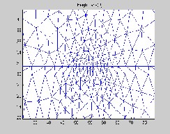
solution domain is discretized into smaller regions called ele- ments, and the solution is determined in terms of discrete val- ues of some primary field variables φ (e.g. displacements in x, y & z directions) at the nodes. The number of unknown pri- mary field variables at a node is the degree of freedom at that node. For example, the discretized domain comprised of tri- angular shaped elements is shown below in Fig. 1. In this ex- ample each node has one degree of freedom.
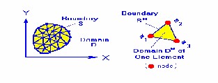
Fig. 1. Typical finite element subdivisions of an irregular domain and typi- cal triangular element.
The governing differential equation is now applied to the domain of a single element (above right). At the element level, the solution to the governing equation is replaced by a conti- nuous function approximating the distribution of φ over the element domain, expressed in terms of the unknown nodal values Φ1, Φ2 and Φ3 of the solution Φ. A system of equations in terms of Φ1, Φ2 and Φ3 can then be formulated for the ele- ment.
Once the element equations have been determined, the ele- ments are assembled to form the entire domain D. The solu- tion Φ(x, y) to the problem becomes a piecewise approxima- tion, expressed in terms of the nodal values of Φ. A system of
IJSER © 2012
http://www.ijser.org
International Journal of Scientific & Engineering Research, Volume 3, Issue 5, May-2012 2
ISSN 2229-5518
linear algebraic equations results from the assembly proce- dure.
For practical engineering problems, it is not uncommon for the size of the system of equations to be in the thousands, making a digital computer a necessary tool for finding the solution. Furthermore, for most practical problems, it is im- possible to find an explicit expression for the unknown, in terms of known functions, which exactly satisfies the govern- ing equations and the boundary conditions. The purpose of the Finite Element Method (FEM) is to find an explicit expres- sion for the unknown, in terms of known functions, which approximately satisfies the governing equations and the boundary conditions. However, the approximate solution may satisfy some of the boundary conditions exactly.
Each region is referred to as an element and the process of subdividing a domain into a finite number of elements is re- ferred to as discretization. Elements are connected at specific points, called nodes, and the assembly process requires that the solution be continuous along common boundaries of adja- cent elements.
2.1 Steps Included in Finite Element Method (FEM)
Theoretically, a Finite Element Method (FEM) analysis is com- posed by four different consequent steps. Those steps are as listed below:
● Discretizing the solution region into finite number of subregion or element.
● Deriving governing equation for a typical element.
● Assembling of all elements in the solution region.
● Solving the system of equations obtained.
In practical terms the Finite Element Method (FEM) analysis
procedure consists of three steps. All of these steps basically,
include four steps mentioned previously. These steps are:
a) Pre-processing. b) Solution. c) Post-processing.
a) Pre-processing: Defining the Finite Element Model
Pre-processing, or model generation, is the most user- intensive part of the analysis. Perhaps up to 90% of the ana- lyst‘s time is taken up creating the finite element mesh. In pre- processing, the analyst defines the geometry and material properties of the structure and the type of element to use. The finite element model, or mesh, is created by defining the shapes of element, the sizes of element and any variation of these throughout the model.
In most modern finite element programs, mesh generation is a two-stage process. The first stage is to create a solid model of the structural geometry in terms of geometrical entities such as points, lines, areas and volumes. Once the geometry is de- fined, the solid model is automatically discretized into a suita- ble finite element mesh using a variety of meshing tools. Usually, the mesh is created to give smaller elements in areas of stress concentration to enhance the accuracy of the solution. Almost all finite element modeling is now done interactive- ly. The analyst either types in commands from a keyboard or selects commands from a menu system using a mouse. The program executes these commands and stores the generated data in a file or database. Graphical representations of points, lines, nodes, elements, etc can then be viewed to ensure the
model definition is correct.
b) Solution: Solving for Displacement, Stress, Strain, etc.
In most of the types of analysis performed the solution proce- dure is linear and straightforward. However, in non-linear problems or problems in which the boundary conditions vary with time (transient analysis) the user must define the loading history and define control parameters for the solution.
c) Post-processing: Reviewing Results in Text and Graphical Form
The results of the analysis are reviewed in the post-processing stage. Finite element programs generate huge amounts of data and it is convenient to use computer graphics to represent the results in graphical form, for example, pictures of the de- formed shape of a structure or contour plots of temperature variation in a thermal analysis.
2.2 Types of Elements
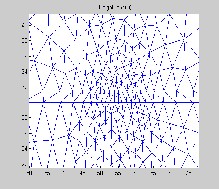
A wide variety of elements types in one, two, and three di- mensions are well established and documented. It is up to the analyst to determine not only which types of elements are ap- propriate for the problem at hand, but also the density re- quired to sufficiently approximating the solution. Engineering judgment is essential. In general, it is a geometrical shape (usually in solid color in modern programs) bounded by dots (nodes) connected by lines. Some solid and shell elements are illustrated in Fig. 2 below.

Fig. 2. A variety of solid and shell finite elements.
3 SILICONE RUBBER INSULATOR
Silicon rubber composite insulators, which are now extensive- ly accepted, did not come out until 1970s, and Germany is the first country developing and using this kind of insulator. Compared to conventional porcelain and glass insulators, composite insulators such as silicon rubber insulator offer more advantages in its application.
Compared with conventional porcelain and glass insulators, composites insulators have the following advantages:
● Light weight.
● High mechanical strength.
● Good electrical performance.
● Excellent Hydrophobicity.
● Small volume.
● Excellent contamination flashover resistant.
● Simple producing art.
● Convenient maintenance.
Hence it is very advantageous to go for Silicon Rubber Insu- lator. So to analyze the characteristics, Silicon Rubber Insulator
IJSER © 2012
http://www.ijser.org
International Journal of Scientific & Engineering Research, Volume 3, Issue 5, May-2012 3
ISSN 2229-5518
is modelled and simulated with different effects.
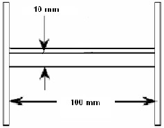
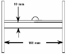
To visualize the effect of a water droplet along silicon rubber
insulator surface, a set up as shown in Fig. 3 is used to simu-
late the electric field and voltage distribution. It consists of a
flat silicon rubber sample of 100mm length and 10mm thick-
ness where it is being connected to electrodes at it ends and
surrounded by air. The live electrode is supplied by 100V
while the water droplet on test is located at the middle of the
silicon rubber sample and it is hemispherical in shape with
5mm radius. Also, the contact angle of the incident water
droplet is set to be 90o. The permittivity of water droplet, sili-
con and air is given by 81, 4.3 and 1 respectively.
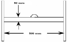
Fig. 3. Set up for analyzing effect of a water droplet on silicon rubber sur- face.
After analyzing the effect of thickness of different dust ma- terial like cement dust, plywood dust, etc. on the insulator surface, it is found that the highest field stress point will move outward. The two types of dusts used to analyze the move- ment of highest field stress point are cement dust and ply- wood dust.
4 SIMULATION RESULTS
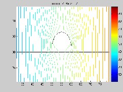
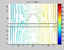
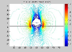
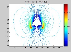
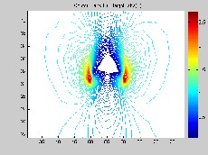
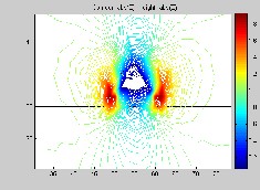
In this study, clean and contaminated conditions were simu- lated using FEM in MATLAB. The Two Dimension of SiR In- sulator under clean and contaminated conditions for FEM Analysis are shown in Fig. 4 and Fig. 5. The results of FEM discretization were shown in Fig. 6 and Fig. 7 respectively. As illustrated in Fig. 8 and 9, water droplets have significant ef- fect on potential and electric field distributions.
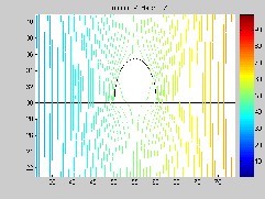
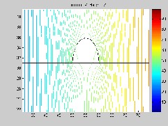
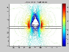
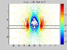
In case of cement dust, increase in the dust thickness has no effect on potential distribution along insulator and dust sur- faces, as illustrated in Fig. 10. No significant difference in po- tential distribution can be seen. In contrast, in case of electric field as in Fig. 11, highest field stress point along insulator surface moves outward from interface point of the water drop- let, air and SiR material as dust thickness increases along SiR surface.
In case of plywood dust contaminated condition, increase in dust thickness has no effect on potential distribution along
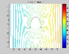
insulator and dust surfaces, as illustrated in Fig. 10. No signif- icant difference in potential distribution can be seen. In con- trast, in case of electric field as in Fig. 11, highest field stress point along insulator surface moves outward from interface point of the water droplet, air and silicon rubber material as dust thickness increases along SiR surface.
Fig. 8 and Fig. 9 display the voltage and field profile respec- tively, surface of silicon rubber without water droplet and surface that comprises one water droplet. Voltage profile of silicon rubber surface without water droplet exhibit a linear relationship while for surface with water droplet, the voltage maintain its magnitude within 49V to 50V along the surface that is directly touched with the water droplets. It is observed that the maximum field stress that occurs along insulator sur- face is 2 V/mm.
Comparison of results illustrated in Fig. 16, 17, 18 & Fig. 19 shows that the highest field stress point moves outward as the dust thickness increases along insulator surface. However in- crease in thickness of dust along insulator surface has no effect on electric potential distribution as shown in Fig. 12, 13, 14 & Fig. 15.
a) W ithout Dust and Water drop
b) W ithout Dust but with Water drop
Fig. 4. Two Dimension of SiR Insulator under clean condition for FEM Analysis.
IJSER © 2012
http://www.ijser.org
International Journal of Scientific & Engineering Research, Volume 3, Issue 5, May-2012 4
ISSN 2229-5518
c) W ith dust but without Water drop d) W ith Dust and Water drop
Fig. 5. Two Dimension of SiR Insulator under contamination on surface for FEM Analysis.
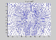
Fig. 6. Finite Element Discretization Results for clean condition.
a) with 0.5 mm cement dust a) with 0.5 mm plywood dust
IJSER © 2012
http://www.ijser.org
International Journal of Scientific & Engineering Research, Volume 3, Issue 5, May-2012 5
ISSN 2229-5518
b) with 1 mm cement dust b) with 1 mm plywood dust
c) with 1.5 mm cement dust c) with 1.5 mm plywood dust
Fig. 7. Finite Element Discretization Results for contamination condition.
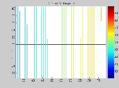

Fig. 8. Potential Distribution under clean condition.
IJSER © 2012
http://www.ijser.org
International Journal of Scientific & Engineering Research, Volume 3, Issue 5, May-2012 6
ISSN 2229-5518
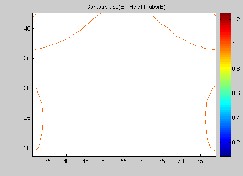
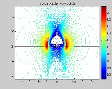
Fig. 9. Electric Field Distribution under clean condition.
a) with 0.5 mm cement dust a) with 0.5 mm plywood dust

b) with 1 mm cement dust b) with 1 mm plywood dust
IJSER © 2012
http://www.ijser.org
International Journal of Scientific & Engineering Research, Volume 3, Issue 5, May-2012 7
ISSN 2229-5518
c) with 1.5 mm cement dust c) with 1.5 mm plywood dust
Fig. 10. Potential Distribution under contaminated condition.
a) with 0.5 mm cement dust a) with 0.5 mm plywood dust
b) with 1 mm cement dust b) with 1 mm plywood dust
IJSER © 2012
http://www.ijser.org
International Journal of Scientific & Engineering Research, Volume 3, Issue 5, May-2012 8
ISSN 2229-5518
c) with 1.5 mm cement dust c) with 1.5 mm plywood dust
Fig. 11. Electric Field Distribution under contaminated condition.
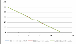
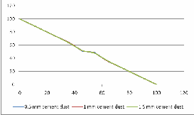
Fig. 12. Electric Potential comparision along cement dust surface.
Fig. 14. Electric Potential comparision along SiR surface with cement dust.
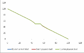
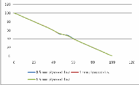
Fig. 13. Electric Potential comparision along plywood dust surface.
Fig. 15. Electric Potential comparision along SiR surface with plywood dust.
IJSER © 2012
http://www.ijser.org
International Journal of Scientific & Engineering Research, Volume 3, Issue 5, May-2012 9
ISSN 2229-5518
Electric Field comparision along sir surface with plywood dust
2.5
2
1.5
1
0.5
0
Electric Field comparision along cement dust surface
0 20 40 60 80 100 120
Leakage Distance(mm)
3
2.5
2
1.5
1
0.5
0
0 20 40 60 80 100 120
Leakage Distance(mm)
0.5 mm plywood dust 1 mm plywood dust 1.5 mm plywood dust
0.5 mm cement dust 1 mm cement dust 1.5 mm cement dust
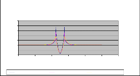
Fig. 16. E values along cement dust surface.
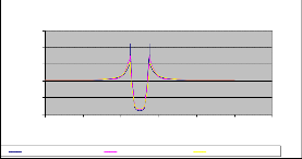
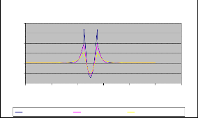
Fig. 19. E values along SIR surface with plywood dust.
3.5
3
2.5
2
1.5
1
0.5
0
Electric Field comparision along plywood dust surface
0 20 40 60 80 100 120
Leakage Distance (mm)
5 CONCLUSION
silicone rubber insulator surface with different thicknesses of dusts were investigated by FEM. As per the results, thickness of contaminants has no effect on potential distri- bution along insulator surface. However, for electric field distribution as the thickness of dust increases, the highest field stress point moves outward along insulator surface from interface point of the water droplet, air and silicon
0.5 mm ply wood dust 1 mm ply wood dust 1.5 mm ply wood dust
Fig. 17. E values along plywood dust surface.
rubber material. The simulation results confirmed good electrical performance of silicone rubber insulator.
REFERENCES
2.5
2
1.5
1
0.5
0
Electric Field comparision along sir surface with cement dust
0 20 40 60 80 100 120
Leakage Distance(mm)
0.5 mm cement dust 1 mm cement dust 1.5 mm cement dust
luted Insulators with Non-Symmetric Boundary Conditions ‘‘,
IEEE Transactions on DEI, Vol. 8, No. 2, April 2001, pp 168-172.
[2] Ailton L. Souza and Ivan J. S. Lopes, ‗‗Electric Field along the Surface of High Voltage Polymer Insulators and its changes under Service Conditions ‘‘, IEEE International Symposium on Electrical Insulation, 2006, pp 56-59.
[3] CIGRE TF 33. 04. 07, ―Natural and Artificial Ageing and Pollution
Testing of Polymer Insulators‖, CIGRE Pub. 142, June 1999.
[4] T. Zhao and R. A. Bernstorf, ―Ageing Tests of Polymeric Housing
Materials for Non – ceramic Insulators‖, IEEE Electrical Insulation
Magazine, Vol. 14, No. 2, March/April 1998, pp. 26 – 33.
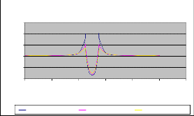
Fig. 18. E values along SIR surface with cement dust.
[5] S. H. Kim, P. Hackam, ‘‘ Influence of Multiple Insulator Rods on Potential and Electric Field Distributions at Their Surface‖, Int. Conf. on Electrical Insulation and Dielectric Phenomena 1994, October
1994, pp. 663 – 668.
[6] B. Marungsri, H. Shinokubo, R. Matsuoka and S. Kumagai, ―Ef- fect of Specimen Configuration on Deterioration of Silicone Ru b- ber for Polymer Insulators in Salt Fog Ageing Test‖, IEEE Trans. on DEI, Vol. 13, No. 1 , February 2006, pp. 129 – 138.
[7] C. N. Kim, J. B. Jang, X. Y. Haung, P. K. Jiang and H. Kim, ―Finite element analysis of electric field distribution in water treed XLPE cable insulation (1): The influence of geometrical configuration of water electrode for accelerated water treeing test‖, J. of Polymer Testing, Vol. 26, 2007, pp. 482 – 488.
[8] L. Donzel, T. Christen, R. Kessler, F. Greuter and H. Gramespacher,
‖ Silicone Composites for HV Applications based on Microvaris-
tors‘‘, 2004 Int. Conf. Solid Dielectrics, Toulouse, France, July 5-9,
IJSER © 2012
http://www.ijser.org
International Journal of Scientific & Engineering Research, Volume 3, Issue 5, May-2012 10
ISSN 2229-5518
2004.
[9] R. G. Olsen, ―Integral Equations for Electrostatics Problems with Thin Dielectric or Conducting Layers‘‘, IEEE Trans. Dielectrics and EI. Insulation, vol. 21, no. 4, pp.565-573, 1986.
[10] U. Van Rienen, M. Clemen & T. Wieland,‖ Simulation of low- frequency fields on high-voltage insulators with light contamina- tions‘‘, IEEE Trans. Magn., vol. 32, no. 3, pp. 816-819, 1996.

Mr. Satheesh Gundlapalli was born in 1978. He is IEEE Member from 2012. He obtained his B.Tech (EEE) degree from JNTUH and M.Tech (PSHVE) from JNTUK, India. He worked as Assistant Profes- sor in VBIT & Associate Professor at TRREC, Hyde- rabad. Presently he is pursuing a Doctoral program at JNT University, Kakinada, India & working as
Asst.Prof. at MRECW, Hyderabad, India. His areas of interest include
High Voltage Insulation Technology and Power System.

Dr. Basavaraja Banakara was born in 1970. He is SMIEEE since 2005. He obtained his B.E. (EEE) degree from Gulbarga University, M.Tech from Karnataka University and PhD from NIT, Wa- rangal, India. He worked as Lecturer, Associate Professor, Professor, Principal and Director Posi- tions at different Institutes/Universities. Present-
ly he is working as a Vice Principal and Professor at GITAM Universi- ty, Hyderebad, India. His areas of interest include Power Electronics and Drives, High voltage Engineering and EMTP applications.

Dr. Pradeep M. Nirgude obtained his B.E. (EE) and M.E. (High Voltage) degrees in 1986 and 1988 from Bangalore and Anna University respectively. He worked as lecturer for about 2 years before joining CPRI in 1989. His areas of interest include High vol- tage testing & measurements, insulation coordina-
tion, diagnostic monitoring of power equipments etc. He has thirty research publications in various National and International conf e- rences. Address: Central Power Research Institute, UHV Research
Laboratory, P.B. No. 9, Uppal, Hyderabad-500039.
IJSER © 2012
http://www.ijser.org