International Journal of Scientific & Engineering Research, Volume 6, Issue 5, May-2015 1091
ISSN 2229-5518
Effect of pyridine and pyridine with substituent on the optoelectronic spectrum of nanoparticles CdS prepared by liquid – liquid interface reaction
Salma M. Shaban, K. T. Al-Rasoul, A. S. Ahmed
Abstract— CdS nanoparticles are prepared by using liquid – liquid interface reaction. from the XRD and TEM analysis we estimated that the size of particles is about 5 nm , which is very comparable with Bohr radius of the CdS ( aB 3 nm ) . The surface are treated through Immersion the powder of nanoparticles on the solution with mix ratio from pyridine and methanol (1:9) for one hour, then the study the UV-
Visible spectrum of the solution. The results indicate a blue shift according to the decrease in the size.
Keywords — CBD, Liquid-Liquid Interface, Nanoparticles.
—————————— ——————————
He relation between the surface chemistry and the elec- tronic properties in semiconductor play a main role when we want to constructed the semiconductor devices, and
for nanoparticles growth the solubility and prevent of aggre- gation of particles can be satisfy through the organic legend which exist in the end of the surface. in the currently research we can notice that there is a big amount of interest about the controlling the electronic properties of nanoparticles semicon- ductor through the use of surface ligands and through the chemical method. A molecules can reacted onto surface of semiconductor and this give us ability to tune the transport of charge carrier [1,2]. It has been found that the nature of ligand layer surrounding semiconductor nanostructure strongly ef- fects on the opto-electronic properties [3].
Pyridine is an aromatic compound with nucleophileic substi- tutions [4], the substituent with pyridine can be divided into two group, the electron donating group EDG which add elec- tron density to the π system making it more nucleophilic and the electron withdrawing group EWG which remove electron density from the π system making it less nucleophilic that de- scribes the affinity of a nucleophile to the nuclei. And note that the Electron-donor groups in the ring increase the reactivity of the N-atom towards electrophiles and the Electron-acceptor groups decrease the N-atom reactivity towards electrophiles. In our work, are used the following from pyridine family [4] Pyridine , 2-methlypyridine ( 2-picoline) , 4-methlypyridine (
4-picoline ) , 2-methoxypyridine ,3-idopyridine , 4-idopyridine
,4-ethlypyridine. Table 1 gives some properties of the previ-
ous material. Also is studied the effect of pyridine and pyri-
dine with substituent on the opto-electronic spectrum of na-
noparticles CdS prepared through the super saturation using
————————————————
• Salma M. Shaban . is currently asist. prof in thin films reacerch lab. in baghdad uneversity , scinece colleage , physics departement , E-mail: sel- mamehdi0@gmail.com
![]()
• K. T. Al-Rasoul is asist prof asist. prof in thin films reacerch lab. in bagh- dad uneversity , scinece colleage , physics departement , E-mail : kmah- di39@yahoo.com
• A. S. Ahmed is currently lecture in thin films reacerch lab. in baghdad
uneversity , scinece colleage , physics departement , E-mail: asaaa- bi@gmail.com
liquid –liquid interface reaction method.
The method to prepare nanoparticles CdS by using liquid – liquid interface reaction need to pass through two steps, the first step is to prepare the precursor which acts as the source of the Cadmium and the second step is the reaction at the in- terface between two immiscible liquid to get a nanoparticle CdS. So in the first step to get the precursor cadmiumdiethyl- dithiocarbamate, we applied the procedure that describe by O'Brien and R.Nomura [5]. In this procedure we dissolve (11 mM) from Sodium hydroxide in 50 ml methanol using a mag- netic stirrer. Then we added (1.128 ml) diethlamine and (0.65 ml) Carbon disulfide. We note that the solution has a pale yel- low. After that and by using the ice bath cooled the solution to
40C for eight hour then added by dropping wisely 50 ml of the methanol which dissolve in it (5.5 mM) from Cadmium Chlo- ride and take it under stirrer for one hour and then note a yel- low solid which represent to produce the precursor then fil- tered and wished by methanol.
then by water and at the last with methanol then dry it by ov- en in the temperature (650-700 c) for 12 hour. In the Second step, worked to prepare the nanoparticles CdS by apply the following steps: at the first dissolve Na2 S in deionized water (
11.46 mg .0.147 mmol ) which consider as the source of sulfide
.then added above it 50 ml of toluene containing 30 mg ( 0.073
mmol.) of cadmium diethyldithiocarbamate. Now noticed two
immiscible liquid one above each other and separated by in-
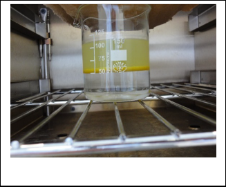
terface layer as shown in the Fig. [1], then put the beaker into
an oven held at 650 C and left it.undisturbed for 24 hour . Att
end of this time, a yellow thin film was found adhered to the
interface of the two liquids.
IJSER © 2015 http://www.ijser.org
International Journal of Scientific & Engineering Research, Volume 6, Issue 5, May-2015 1092
ISSN 2229-5518
then left it for one houre ,then measure the UV-Visible absorb- ance of the solution .
From the X-ray diffraction pattern for nanoparticles CdS with- out any surfactant added, which obtain in Fig. 2, note that we have peaks at 2θ can be assigned to [002], [110], [112] planes of hexagonal CdS. And can note that the peak at 2θ=25.590,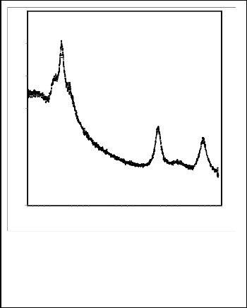
2θ=42.50, and 2θ=51.130 attributed to the [002] for hexagonal structure or [111] for cubic, the [110] for hexagonal structure or [220] for cubic the [112] for hexagonal structure or [311] for cubic respectively. But the peak at 24.930 are purely indicate to [100] for hexagonal structure. we consider that the deposited consists of both the cubic and hexagonal forms. Such mixed phases have been previously reported in chemically deposited CdS nanostructures [6-10]. And note that the producer is free from crystalline impurities.
Fig. 1. Two immiscible liquids to get the interface reaction for nanoparticles CdS.
600
The procedure of the previous steps can be explain in the fol- lowing equation:
NaOH + CSR2R+HNɛtR2 R ![]() Na (SR2RCN ɛtR2R) + HR2RO After cooling added Cadmium Chloride and get the following
Na (SR2RCN ɛtR2R) + HR2RO After cooling added Cadmium Chloride and get the following
reaction:
Na (SR2RCNɛtR2R) +CdClR2 R![]() Cd (SR2RCN ɛtR2R)2+ 2NaCl
Cd (SR2RCN ɛtR2R)2+ 2NaCl
In this step, get the precursor Cd (S2CNEt2)2 which can be
used in the following steps to produce nanoparticle CdS as:
At the first we dissolved Na2S in deionized water as shown in the following equation:
NaR2RS + HR2RO =NaOH+HR2RS
Then HR2RS dissociated according to the following equation : 0
20
HR2RS = H +HS
2θ (Degree) 55
And at last HS dissociated as in the equation
HS-=H++S-2
All these done in an aqueous solution for NaR2RS, so the last re- sult is the H+ and S -2 when layered the toluene above the aqueous solution which contain the Cd (SR2RCN ɛtR2R)R2R. The fol- lowing reaction act in the interfacial layer which separated the two solutions
Fig. 2. X-ray diffraction patterns obtained for nanoparticles CdS using the interface reaction for the system of H2O – Toluene.
(SR2RCN ɛtR2R)R2R (if) + S
(if) ![]() CdS(if)+(SR2RCN ɛtR2R)2-2(ol)
CdS(if)+(SR2RCN ɛtR2R)2-2(ol)
2Na (aq) +1 + (S2CN E ɛt )![]()
(if) -2 Na2 (S2CN Et2)
(aq)
Immerse 0.1 gm from powder of nanoparticles CdS in the solution which consist of 1 ml of pyridine in 9ml of methanol ,
IJSER © 2015 http://www.ijser.org
International Journal of Scientific & Engineering Research, Volume 6, Issue 5, May-2015 1093
ISSN 2229-5518
TABLE1
THE PARAMETERS FROM X-RAY DIFFRACTION PAT-
TERN![]()
2θ (Deg.) | d hkl Exp.(Å) | d hkl Std.(Å) | phase | hkl | card No. | |
24.93 | 3.5688 | 3.5808 | Hex. | (100) | 96-900-8863 | For actual size of grains, the broading of the peaks may be |
25.59 | 3.4782 | 3.3745 | Hex. | (002) | 96-900-8863 | caused by residual stresses. Stresses within the crystal cause |
3.3544 | Cubic | (111) | 96-101-1252 | corresponding strains, which result in a planar spacing and shifting the peaks. Often residual stresses produce a combina- | ||
42.50 | 2.1253 | 2.0674 | Hex. | (110) | 96-900-8863 | tion of compressive and tensile strains. In order to calculate |
2.0541 Cubic (220) 96-101-1252
52.13 1.7531 1.7629 Hex. (112) 96-900-8863
1.7518 Cubic (311) 96-101-1252
the average crystallite size including strain, adopted the Wil-
liamson –Hall method [11,12] where the strain (ɛ) and crystal-
lite size (L) are related to the measured β following the equa-
tion:![]()
The broadening of the peaks indicating that we have a na- noscale of the size. The grain size of the particulates can be estimated using Scherer equation:
d= 0.9 λ / β cos θ (1)
Where β is the full width at half maximum in radians, λ is the wavelength of X-ray used and θ the angle of diffraction. And when apply this relation for the diffraction angle in Fig. 2,
β cos θ / λ = 1/L + ɛ sin θ / λ ( 2)
Where β, λ and θ are the full-width at half maximum (FWHM) of the diffraction peaks, wavelength of the x-ray source and Bragg's angle respectively. For this calculation, the most prom- inent peaks as shown in the inset of Fig. 2 were analyzed. Fig.
3 represents the plot of (β cos θ / λ) versus sin θ / λ) which is a straight line. The slope of the plot gives the amount of residual strain, whereas reciprocal of intercept on the y-axis give the average particle size. Values 1.56*10-2 and 10.4 nm are ob- tained for strain and average grain size, respectively.
TABLE2
VALUES OF GRAINS SIZE FROM X-RAY DIFFRACTION
![]()
PATTERN
nanoparticles Cds
y = 0.0156x + 0.0961
gree)![]()
FWHM (degree)
size
(nm)
0
1 Sin θ /λ 3
25.59 1.1949 7.6
42.5 1.0584 8.9
52.13 1.6482 5.9![]()
when are compare with Bohr radius we note that it is in the range of nanoparticle (two or three multiple of Bohr radius or in the range (2-10) nm. Table 2 indicates the calculation of val- ue of grains size using Scherer equation.
Fig. 3. W illiamson –Hall plot to determine the particle size and strain of nanoparticles CdS
IJSER © 2015 http://www.ijser.org
International Journal of Scientific & Engineering Research, Volume 6, Issue 5, May-2015 1094
ISSN 2229-5518
TABLE3
Value of (β cos θ / λ ) and ( sin θ / λ) to apply Williamson –Hall
method
imum ( FWHM) are obtained using the first derivative of the curve as shown in Fig. 5
2θ | β deg | β Rad | λ nm | sin θ / λ | β cos θ / λ |
26.50 | 1.1459 | 0.01998 | 0.15406 | 1.5 | 0.126 |
43.60 | 1.0306 | 0.01797 | 0.15406 | 2.53 | 0.108 |
51.90 | 1.5872 | 0.02768 | 0.15406 | 2.85 | 0.1615 |
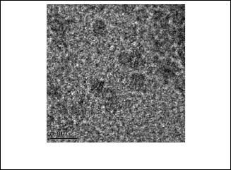
Transmission electron microscopy gives us more detailed about the structure. From the picture that results from trans- mission electron microscopic, notice that the Individual grains making up the platelets can clearly resolved, especially at high resolution. Lattice fringes corresponding to the spacing be- tween (110) and (002) planes of hexagonal CdS are clearly seen in figure 4. The long edge of grains is typically around 3 nm.
Fig. 5. Exhibits: (a) Electronic absorption spectrum of CdS
nanocrystalline thin film, (b) Gaussian fitting of the spectra the
CdS nanocrystalline thin film [7].
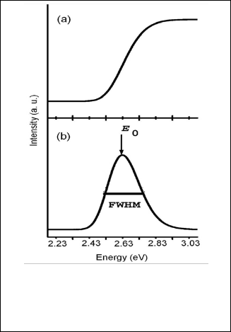
The UV absorption spectrum for CdS is shown in Fig. 6a. Dif- ferentiation of this absorption spectrum yields the curve shown in Fig. 6b. In order to obtain the position of absorption maxima, Gaussian function fitting of absorption spectra was performed, as shown in Fig. 6b. To apply this method, the po- sition of the peak energy E0 is obtained using the first deriva- tion of the curve. The E0 is translated as d [5-8] by usiing the formula
Fig. 4. Transmission electron microscopic images of nanoparticles CdS.
∆Eg =1/ad2+bd+c ( 4)
Where a, b and c are constants that depend on the identity of
the semiconductor; for CdS their values are 0.1278, 0.1018 and
0.1821 respectively. Here, ∆Eg is the observed shift in the band
gap (Eg) given by E0 – Eg..
To estimate the energy gap and the size can be used tight binding approximate (gaussing fitting). This is model was de- rivative by D.D Sarma and co-workers which is used to calcu- late of band gap of colloidal sols [13,14]. To apply this method, the position of peak ( E0) , as well as its full width at half max-
IJSER © 2015 http://www.ijser.org
International Journal of Scientific & Engineering Research, Volume 6, Issue 5, May-2015 1095
ISSN 2229-5518
0.4
CdS Experemental
Gaussian fitting
2 CdS+4 ethlypyridine
Experemental
Gaussian fitting
0
1.5 4
E (eV)
0
1.5
E (eV) 4
Fig. 8. Gaussian fitting for( dA/dE ) 2 as a function for EeV for nanoparticles CdS / 4-ethlypyridine
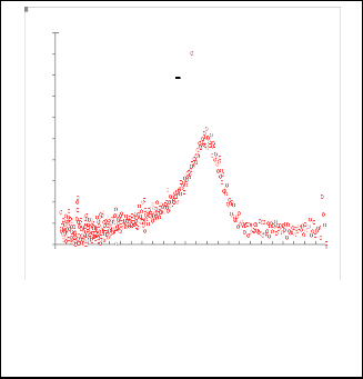
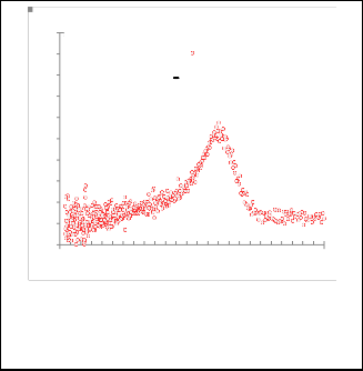
Fig. 6. Gaussian fitting for ( dA/dE ) as a function for E (ev) for nanoparticles CdS.
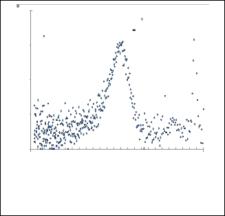
1 CdS+pyridine Experemental Gaussian fitting
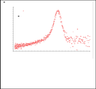
1 CdS+2 picoline
Experemental
Gaussian fitting
0
1.5
E (eV) 4
0
1.5
E (eV) 4
Fig. 7. Gaussian fitting for( dA/dE ) as a function for EeV for nanoparticles CdS / pyridine.
Fig. 9. Gaussian fitting for( dA/dE ) 2 as a function for EeV for nanoparticles CdS / 2-picoline.
IJSER © 2015 http://www.ijser.org
International Journal of Scientific & Engineering Research, Volume 6, Issue 5, May-2015 1096
ISSN 2229-5518
1 CdS+4 picoline
Experemental
Gaussian fitting
1 CdS / 2-methoxypyridine
Experemental
Gaussian fitting
0
1.5
0
E (eV) 4
1.5
E (eV) 4
Fig. 13 Gaussian fitting for( dA/dE ) 2 as a function for EeV for
nanoparticles CdS+2-methoxypyridine.
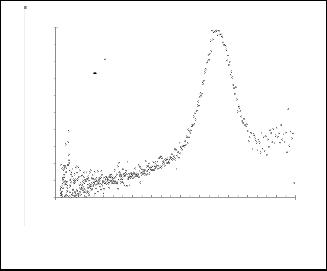
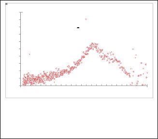
Fig. 10. Gaussian fitting for( dA/dE ) 2 as a function for EeV for nanoparticles CdS / 4-picoline.
1 CdS / 4-idopyridine
1 CdS / 3-idopyridine
Experemental
Gaussian fitting
Experemental
Gaussian fitting
0
1.5
E (eV) 4
0
1.5
E (eV) 4
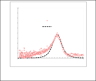
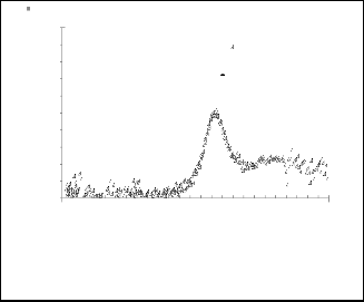
Fig. 12 Gaussian fitting for( dA/dE ) 2 as a function for EeV for nanoparticles CdS/3-idopyridine.
Fig. 11 Gaussian fitting for( dA/dE ) 2 as a function for EeV for nanoparticles CdS/4- idopyridine.
IJSER © 2015 http://www.ijser.org
International Journal of Scientific & Engineering Research, Volume 6, Issue 5, May-2015 1097
ISSN 2229-5518
We must know that for nanoparticles CdS after reacted with pyridine , this indicate that the nitrogen atom in pyridine is
TABLE4
![]()
THE PYRIDINE AND PYRIDINE W ITH SUBSTITUENT EFFECT ON THE NANOPARTICLES CDS
nucleophilic because the lone pair of electrons on nitrogen cannot be delocalized around the ring. For CdS nanoparticles whose structure is similar to a strong electrolyte have Cd+2 rich surface is capped and bound to surface by the electrically neutral ligand pyridine as shown in the figure.[14,15]
∆Pka
Pka RpyridineR –Pka
Rpyridine +substituentR )
------ positive
positive positive
0 negative
negative negative
Effect of
substituent
on the pyr- idine ring
------
EDG EDG EDG
----- EWG EWG EWG
Eg (eV)
2.8
3.05
3
2.95
2.9
3.2
2.95
2.9
d (nm)
3.9
2.9
3
3.2
3.4
2.5
3.2
3.4
Fig. 14 the bond between the pyridine and nanoparticles
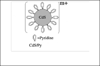
CdS[15].
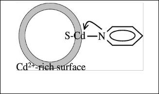
Fig. 15 the reaction between pyridine and nanoparticles CdS [15]
.
From Table 4, the Pka value relates to electron density of ni- trogen atom in the pyridine ring [16] and this represent to strength of reaction with nanoparticles, so when pyridine re- acted with nanoparticles it reacted with surface of these parti- cles and this make surrounding layer insulator for these parti- cles from others and prevent them to aggregation, so at the first, notes that the energy gap of all samples increase which represent to the decrease in size and then depend on the Pka to note amount of this change , so when substituent belong to the electron donating group we notice that the change in band gap is small and decrease with the increase the pka which may be means that the ability to aggregation depend on the elec- tron density of nitrogen atom , on the other hand, notice that the band increase with decrease the Pka of the substituent when belong to the electron with drawls group and this may returns to the reduce of electron density of nitrogen on the acclamation of particles.![]()
nanoparticles CdS prepared using liquid -liquid interface reac- tion , the size is comparable to the Bohr radius of CdS , and this estimated through XRD , TEM , and UV-Visible analysis. for estimated the nanosize and the energy gap from UV- Visible spectrum we use the model that derivative by Samara at el. which give us much accurate result . in our work we aim to study the effect of pyridine and pyridine with substituen familly on the opto-electronic spectrum of the nanoparticles CdS through the reacted with the surface of these particles , and we reach that there is an increase in the energy gap for all samples which mean that there is a change in the size accord- ing to the substituen in the pyridine ring . and we reach this chang depend on the electron density on the niterogen atom in the pyridine ring and this density of electron can be esti- mated from Pka value.
[1] A. Vilan, A. Shanzer, and D. Cahen. " Molecular control over
Au/GaAs diodes"Nature " , Vol .404, pp.166-168 ,2000 .
[2] R. Cohen, L. Kronik, S. Shanzer, D. Cahen, A. Liu, Y. Rosenwaks, J. K. Lo renz, and A. B. Ellis. , " molecular control over semiconductor surface elec tronic properties : dicarboxylic acids on CdTe , CdSe,GaAs and InP " , " J. Am. Chem. Soc"., Vol.121, pp 10545 , 1999.
[3] M. Kuno, J. K. Lee, B. O. Dabbousi, F. V. Mikulee, and M. G.
Bawendi. " The band edge luminescence of surface modified CdSe nanocrystallites: Probing the luminescing state " , " J. Chem.Phys. " , Vol. 106, pp. 9869 , 1997.
[4] A. Rauk , Orbital Interaction Theory of Organic Chemistry, chapter 11 , page
11 , Second Edition , Copyright ( John Wiley & Sons, Inc., (2001).
[5] P.O'Brien and Nomura, " Single-molecule precursor chemistry for the deposition of chalcogenide (S or Se)-containing compound semicon ductors by MOCVD and related methods " , J.Mater.Chem. 5, pp. 1761
,1995.
[6] P.Thomas, p.O'Brien., " Deposition of nanostructured films of CdSe and
CdS using three layered water–oil–amphiphile/salt system. " , "
j.Mater.Chem.C, 1, pp.671 ,2013.
IJSER © 2015 http://www.ijser.org
International Journal of Scientific & Engineering Research, Volume 6, Issue 5, May-2015 1098
ISSN 2229-5518
[7] D. Kim, Y. Yu, J. Lee and Y. Ghoi, " INVESTIGATION OF ENERGY BAND GAP AND OPTICAL PROPERTIES OF CUBIC CDS EPILAYERS " , " Appl. Surf. Sci., Vol. 254, pp 7522 , 2008.
[8] S.Ramaiah,R.Pilkington,A.Hill,R.Tomlinson and A.Bhatnagar, " Struc
tural and Optical Investigation on CdS Thin Films Grown by Chemi-
cal Bath Technique " , " Mater.Chem.Phys." Vol . 68, pp. 22 -30
,2001.
[9] S.Mahanty,D.Basak,F.Rueda and M.leon, " optucal properties of chemical bath deposited CdS thin films " , " J.electron.Matter" , Vol. 28, pp. 559-562
,1999.
[10] Y.Lo,R.Choubey,W.Yu,W.Hsu and C.Lan, " shallow bath chemical deposi
tion of CdS thin film " , " Thin Solid Films. " , Vol. 520, issu . 1 pp. 217-223 ,
2011
[11] G.Cao,Nanostructure and Nanomaterials,1st ed., Imperial College
Press,London, (2004).
[12] G.K.Williamson,W.H.Hall, " X-ray line broadening from filed alumin
ium and wolfram L'elargissement des raies de rayons x obtenues des limailles d'aluminium et de tungstene Die verbreiterung der roent geninterferenzlinien von aluminium- und wolframspaenen " , "Acta Metal " , l. (1953) 122-31.
[13] S.Sapra and D.D.Sarma , " Evolution of the electronic structure with
size in II-VI semiconductor nanocrystals " , " Phys . Rev. B: Condens. Mater.Phys." , 69, (2004) 125304,
[14] D.Talapin,J.Lee,M.KovalenkoandE.Shevehenko, " prospects of colloidal nanocrystals for electronic and optoelectronic application " , " Chem.Rev." , Vol 10 , issu . 1 pp. 389 - 458 , 2010.
[15] Yu Zhang, Xin Wang, Ming Ma, Degang Fu, Ning Gu, Juzheng Liu, Zuhong Lu, Yi Ma, Ling Xu, Kunji Chen, " Influence of surface- capping molecule exchange on the hyper-Rayleigh scattering of CdS nanoparticles" , " Applied Surface Science ", vol. 205, issu 1-4 . pp.
256–261., 2003
[16] S. Saieed and A. Najim , " Effect of Atomic Charge and Some Physical
Properties on pKa of Substituted Pyridines " , " J. Edu. & Sci. " , Vol
. 24, No. 4 , pp 25-33 ,2011 .
IJSER © 2015 http://www.ijser.org