International Journal of Scientific & Engineering Research, Volume 5, Issue 2, February-2014 268
ISSN 2229-5518
Economic Handheld Electronic Traffic Challan
System
Dinesh Nagar, Amit Sharma
Abstract— These The Economic handheld Electronic Challan System is most suitable for traffic police to make Challan and store the rec- ords on EEPROM (Electrically Erasable Programmable Read Only Memory). In this paper we have developed a system in which the details re- lated to Challan is entered by keyboard , displayed on LCD and the thermal printer will print the Challan .This details will be stored in the memory and displayed on LCD(Liquid crystal display) . This system is based on P89V51RD2 microcontroller. Embedded C language is used for development of the system software. The real time date and time is taken by using RTC (Real Time Clock) and data is stored in EEPROM .I2C protocol used for communication between RTC and P89v51rd2. ORCAD schematic software is used for designing the circuit and PCB for this system.
Index Terms— P89V51RD2, I2C, EEPROM, Real Time Clock, I2C, Thermal Printer, keybord.
—————————— ——————————
MBEDDED system is used in more and more applications today. Embedded system require very less amount of power and small in sizes so that one can carry it easily. The economic
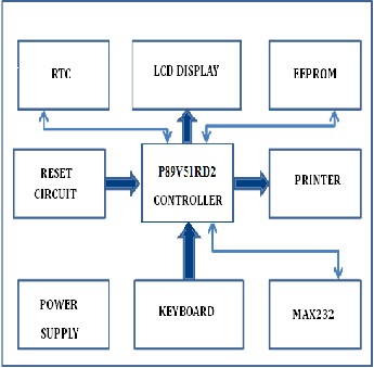
handheld traffic challan system is based on P89V51RD2.This microcon- troller is the heart of this system. The feature of the P89V51RD2 is its X2 mode option. The design engineer can choose to run the application with the conventional 80C51 clock rate (12 clocks per machine cycle) or select the X2 mode (6 clocks per machine cycle) to achieve twice the throughput at the same clock frequency. The Flash program memory supports both parallel programming and in serial In-System Programming (ISP). Parallel programming mode offers gang-programming at high speed, reducing programming costs and time to market. ISP allows a device to be repro- grammed in the end product under software control. The P89V51RD2 is also In-Application Programmable (IAP), allowing the Flash program memory to be reconfigured even while the application is running. W e have interfaced the RTC, hex keyboard ,LCD and Thermal Printer with micro- controller.
The basic block diagram is shown in figure 1.
————————————————
• Dinesh Nagar is currently working in Engineering College Tuwa, Godhra (GJ) India as Assistant Professor in Electronics and Communication Engi- neering Department. E-mail: dineshnagar7784@gmail.com

Figure 1. Basic Block Diagram
The challan system is designed in such a way that when- ever the challan is prepared the person will select the fine type that is whether no license card or no registration card or no insurance or breaking traffic rules. After selecting the proper fine type the vehicle number and license number is entered with the help of keyboard. In the software func- tions enter_licence_no(); and enter_vehicle_no(); is used to enter this details .The LCD(Liquid crystal display) display will show the next step that is confirm and print .The func-
IJSER © 2014 http://www.ijser.org
International Journal of Scientific & Engineering Research, Volume 5, Issue 2, February-2014 269
ISSN 2229-5518

tion void print_details() is used for printing .
Start
Fine type Lcense/registrat ion/breaking
YES
NO
Enter License no.
Enter Vehicle no.
Confirm and print
End
puter and pressing retrieve key from the keypad of the device. Pass word can be assigned to enter during this process. It is also possible to erase all the data from the memory of the de- vice by pressing a single button and entering password if pro- grammed for it.
enter_licence_no(); enter_vehicle_no(); print_details(); store_details_into_eeprom();
Printers are routinely classified by the technology they em- ploy; numerous such technologies have been developed over the years. The choice of printer has a substantial effect on what jobs a printer is suitable for.
Thermal printer is more suitable for our application. Printer is primarily used as local peripheral, and is attached through serial interface to a microcontroller which serves as a docu- ment source.
Thermal printers work by selectively heating regions of spe- cial heat-sensitive paper. Colors can be achieved with special papers and different temperatures and heating rates for differ- ent colors; these colored sheets are not required in black-and- white output.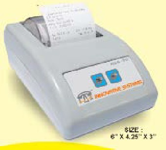
Figure 2. Traffic Challan System flowcharts
Supply circuitry provides necessary power to the device. When the device is powered on, it displays a default home screen. On pressing the new session button from the keypad. It will ask for the license number after entering the number device will ask for the vehicle number, and after that it will displays the menu for the previously defined fine types for the violation of traffic rules. After selecting all fine types to be paid, on pressing the OK button it will finally displays the all the details of the current session and total amount fined to the driver. Then print button is to be pressed to take the final print from the printer.
All these processes are centrally controlled by the microcon- troller. The time details associated with the session is obtained from the RTC. All the details for all the sessions are stored in the EEPROM in the device.
At the end of the duty of the concerned person, de- tails for all the sessions are retrieved from the memory (EEPROM) of the device by serially connecting it to the com-
Figure 3. Thermal Printer
For the IC’s interconnections, designers often first select com- ponents supporting I2C (Inter-IC). Here I2C is utilized to in- terface RTC (Real Time Clock) and EEPROM.
The I2C bus, a simple Master-Slave serial bus architecture uti- lizes only a 2-wire connection. A serial data line, SDA, is used to transmit data to and from slaves. A single serial clock, SCL, generated by the master and is used to clock data in or out of slave devices. The I2C bus uses a simple protocol. The Master
IJSER © 2014 http://www.ijser.org
International Journal of Scientific & Engineering Research, Volume 5, Issue 2, February-2014 270
ISSN 2229-5518
transmits the Slave Address and a Read or Write bit to indi- cate the direction of transfer.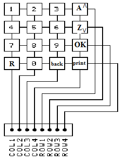
A device read is performed by performing a device write writ- ing the Slave followed by the address of the memory location of register. A device read is then performed and the device remembers the internal offset previously set and the read re- turns the byte requested either a register or memory location. If an ACK is sent rather than an NACK the slave device can then auto increment the pointer and read the next location until the master sends a NACK. I2C is a very useful IC inter- face when accessing device registers, memory and peripherals are important. The biggest advantages of I2C are it is widely supported, well known, can be used as a cable connection over longer distances.
The DS1307 is a low-power clock/calendar with 56 bytes of battery-backed SRAM. The clock/calendar provides seconds, minutes, hours, day, date, month, and year information. The DS1307 operates as a slave device on the I2C bus. When device turned off, the device switches into a low-current battery- backup mode. Thus battery keeps RTC clock alive even in the off mode of the device.
The AT24C164 provides 16,384 bits of serial electrically erasa- ble and programmable read only memory (EEPROM) orga- nized as 2048 words of 8 bits each. The device’s cascadable feature allows up to eight devices to share a common 2-wire bus. The device is optimized for use in many industrial and
commercial applications where low power and low voltage operation are essential.
The HEX keypad is connected with microcontroller for enter- ing the details .in this each square with a number or letter in it is a push to make switch, which connects the horizontal wires (rows) with the vertical wires (columns). So if you press but- ton '1' it will connect COL1 with ROW1, or pressing button '6' will connect COL3 with ROW2. For a numeric (4x3) keypad COL4 will be missing, and 'A' and 'B' replaced with '*' and '#' but is otherwise the same. The sample programs use a lookup table for the keys; this would need to be changed to insert the correct values for the non-numeric characters.
As the switches are all interconnected, we need a way to dif- ferentiate between the different ones - the four resistors on the interface board pull lines COL1 to COL4 high, these four lines are the ones which are read in the program. So in the absence of any switch been pressed these lines will all read high. The four ROW connections are connected to output pins, and if these are set high the switches will effectively do nothing - connecting a high level to a high level, results in a high level.
In order to detect a switch we need to take the ROW lines low, so if we take all the ROW lines low. Assuming we press button 1, this joins COL1 with ROW1, as ROW1 is now at a low level, this will pull COL1 down resulting in a low reading on COL1. Unfortunately if we press button 4, this joins COL1 with ROW2, as ROW2 is at a low level this also results in a low reading at COL1. This would only give us four possible choices, where each four buttons in a COL do exactly the same (e.g. 1, 4, 7, and A are the same). The function used in the sys- tem is unsigned char keyboard ().
Figure 4. Hex Keypad
The Microcontroller used in this system is NXP P89V51RD2. It belongs to the 8051 family of microcontrollers. Some ad- vantages of using P89V51RD2 are [4]–
• 80C51 Central Processing Unit
• 5 V Operating voltage from 0 to 40 MHz
• 64 kB of on-chip Flash program memory with ISP (In- System Programming) and IAP (In-Application Pro- gramming)
• Supports 12-clock (default) or 6-clock mode selection via software or ISP
• SPI (Serial Peripheral Interface) and enhanced UART
• PCA (Programmable Counter Array) with PWM and Cap- ture/Compare functions
• Four 8-bit I/O ports with three high-current Port 1 pins
(16 mA each)
• Three 16-bit timers/counters
• Programmable Watchdog timer (WDT)
• Eight interrupt sources with four priority levels
• Second DPTR register
• Low EMI mode (ALE inhibit)
• TTL- and CMOS-compatible logic levels
The complete circuit diagram is designed in ORCAD software.
IJSER © 2014 http://www.ijser.org
International Journal of Scientific & Engineering Research, Volume 5, Issue 2, February-2014 271
ISSN 2229-5518
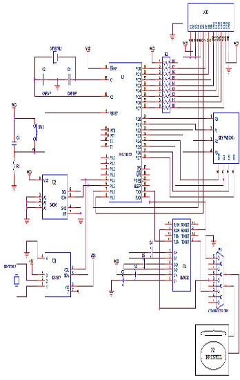
Figure 5. Circuit Diagram for Traffic Challan System
The main objective behind of this paper is to introduce small scale device development methodology on real time platform.
We would like to thanks our principal and college manage- ment for carring out this work, also thanks to my friend Mr. Nirav patel for his cooperation in this work.
[1] Jean Marc Irazabal and Steve Blozis, “The I2C Bus Specification”, Version 2.1, Jan 2000, Philips Semiconductor. Programming,
07/31/2001
[2] David Kalinsky and Roee Kalinsky, “Introduction to I2C”, Embed- ded Systems
[3] “DesignCon 2003 TecForum I2C Bus Overview January 2003”,
Philips Semiconductors
[4] S. Akash,Bibek Kabi , Mr. S.Karthick , “Implementing a Line Tracing
Robot as an effective Sensor and Closed Loop system” , IJRTE ,Vol2
,No.7,November 2009
[5] Vijay Kumar Singh and Sindhu Hak Gupta, “PIC based Data Acquisi- tion System using Bluetooth” ,978-1-4244-8541-3/10/$26.00 ©2010
IEEE
[6] Mazidi,”The 8051 Microcontroller And Embedded Systems Using
Assembly And C”, Edition, 2. Publisher, Pearson Education, 2007
IJSER © 2014 http://www.ijser.org