International Journal of Scientific & Engineering Research, Volume 6, Issue 4, April-2015 918
ISSN 2229-5518
Design of a High Speed Adder
Aritra Mitra, Amit Bakshi, Bhavesh Sharma, Nilesh Didwania
Abstract— In this paper we have compared different addition algorithms such as Ripple Carry Adder, Carry Save Adder, Carry Select Adder, Carry Look Ahead Adder & Kogge Stone Adder for different performance parameters i.e. Area Utilization, Speed of operation and Power Consumption. A high speed Adder is then designed by merging Kogge Stone & Carry Select Algorithms. The circuits have been designed using Verilog HDL & Synthesize using TSMC 180 nm standard cell. The performance parameters are obtained with the help of Cadence Encounter RTL Compiler.
Index Terms Adder, Carry Select Adder, Kogge Stone Adder, Verilog HDL.
—————————— ——————————
1 INTRODUCTION
dder Circuits are the most basic block of any digital system. In any arithmetic function addition plays a role of most fundamental operation. Adders are commonly
used in miscellaneous application in modern VLSI system like multiplier design, design of an ALU, and also in various Digital Signal Processing algorithms like FIR, IIR Filter design. Designing an excellent and efficient of an adder circuit a designer must optimize the parameters like area, delay, and power. We have to tradeoff between all three parameters to get an efficient design. Depending upon the need and application some changes and compromises have to be made [1].
In modern VLSI design era delay in data path considered as a crucial parameter these days. Designers are trying to minimize the delay as the speed up operation becomes faster [2]. There has been lot of researches and work regarding minimizing of delay and now designer look for making an adder circuit which is efficient and significantly faster.
2 ADDER ARCHITECTURE
2.1 Ripple Carry Adder
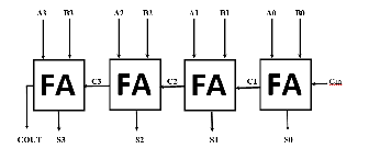
Ripple Carry Adder (RCA) is considered as the most Simplistic approach among all the addition algorithms. A N- bit Ripple Carry Adder requires N number of full adders [4]. It is basically a Cascading formation of full adders in series. As a full adder block process three inputs along with carry bit and produce two outputs i.e. Sum bit and Carry-out Bits, the Carry of one full adder block acting as a carry in for the next full adder.
In this paper few basic adder like Ripple carry adder, Carry Save Adder, Carry look-ahead Adder, Carry Select Adder & Kogge stone adder have been made using Verilog HDL and then it’s parameters are obtained using Cadence Encounter RTL Compiler[3]. After that we have merged two of these algorithms to reduce the delay in data path. We made a kogge-stone based Carry Select Adder which delivers a much faster speed of operation than the other adder circuitry.
————————————————
• Aritra Mitra is currently pursuing dual degree program in Electrics & Tele communication engineering in KIIT University, India, PH-
+918093944635. E-mail: Aritra.mitra000@gmail.com
• Amit Bakshi is currently Assistant professor of KIIT University, India,
E-mail: abakshi.ece@gmail.com
• Bhavesh Sharma is currently pursuing dual degree program in Electrics &
Tele communication engineering in KIIT University, India.
• Nilesh Didwania is currently pursuing dual degree program in Electrics &
Tele communication engineering in KIIT University, India.
Fig. 1. Block Diagram of 4 bit Ripple carry adder
The Sum bit and the carry bit will be calculated as follows
Sn = An^Bn^Cn-1 (1)
Cout = ((An . Bn) + (Bn . Cn-1) + (An . Cn-1)) (2)
2.2 Carry Save Adder
Another Algorithm for faster calculation of Addition is Carry Save Adder. It is also same as full Adder. From the two inputs we first produce two temporary Outputs named as Sum and Carry. For getting sum bit we first perform bitwise XOR and for the Carry bit we execute bitwise AND for the two input numbers. And then finally add them by shifting Carry bit left by one place to Sum bit up to produce final answer [4].
IJSER © 2015 http://www.ijser.org
International Journal of Scientific & Engineering Research, Volume 6, Issue 4, April-2015 919
ISSN 2229-5518
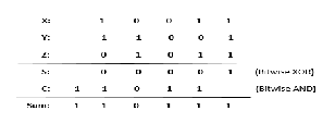
Fig. 2. Working of Carry Save Adder (CSA)
2.3 Carry Look Ahead Adder
Another fast addition topology is Carry Look Ahead Adder. The main advantage of Carry Look Ahead Adder over Ripple Carry Adder is it improves the speed of operation by reducing the time needed to determine the carry bits. Carry Look Ahead adder calculate the sum and carry simultaneously by using a separate carry generation unit[5].
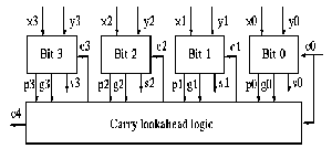
Fig. 3. Working of Carry Look Ahead Adder (CLA)
First a propagation and generation signal is made using the input bits. i.e.
P(x, y) = X ^ Y (3) G(x, y) = X . Y (4) And all the carry are generated simultaneously by this formula
C = G + P.Cprev. (5) Finally the sum bit is calculated by xor-ing the Propagation bit and its previous stage carry bit.
2.4 Carry Look Ahead Adder
Carry Select Adder algorithm is nothing but calculating sum by guessing the carry input which we will be getting from previous stage.
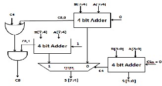
Fig. 4. Working of Carry Select Adder (CSLA)
Two adder work simultaneously in this adder algorithms where one is calculating sum by taking carry input as 0 from the previous stage and the other adder does so by taking Carry bit as 1[4]. Several multiplexer is used to choose the appropriate sum bit corresponding to its previous carry out bit [6].
2.5 Kogge Stone Adder
Kogge Stone adder is the parallel prefix Adder and broadly considered as one of the fastest addition method. Carry generation is much faster because of parallel computation [7]. The Kogge Stone adder comprises of three stages like Pre- processing Stage, Carry generation Stage and Post-Processing Stage. In the pre-processing stage propagation and generation signals are generated. Carry Generation Stage includes several Black Cells and Grey cells which used to generate carry for the next stages and finally Post-processing Stage is used to generate Sum and carry out bit.
From the pre-processing stage we get P(a,b) and G(a,b)
signals.
P(a, b) = A ^ B (6)
G(a, b) = A.B (7)
From the Carry Generation Stage we get the Black cell and
Grey Cells. The equations for those are
G black = (Gprev . P) + G (8)
P black = (P . Pprev ) (9)
G grey = (Gprev . P) + G (10)
Sum and Carry out bit is generated in the Post-Processing
Stage.
Sn = ( Pn ^ Cn-1 ) (11)
Kogge stone adder is one well known faster addition technique and also has a lower fan-out at the output which increases its performance but on the other hand, it occupies much area and creates wiring congestion problem.
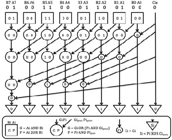
Fig. 5. Working of Kogge-Stone Adder (KSA)
IJSER © 2015 http://www.ijser.org
International Journal of Scientific & Engineering Research, Volume 6, Issue 4, April-2015 920
ISSN 2229-5518
3 Modified Adder
Now we have merged two of the above mentioned addition technique in order to generate a new modified architecture for addition. We have used both Carry Select and Kogge Stone Addition method and generated an addition technique which is much faster than the others. In conventional carry Select adder we have been used Ripple Carry adder for calculating the Upper and Lower nibble. But use of Ripple carry adder will subsequently increase the delay as the carry generated by one full adder will ripple through the next stage where as the Kogge stone adder reduces much amount of delay in the data path.
Suppose for an 8 bit Carry Select Adder method, the modified architecture adds its first two bit using Kogge Stone adder instead of using Ripple Carry Adder. Then rest 6 bits are sub divided into three blocks and each block has been calculated twice assuming a carry in bit of 0 and 1 respectively. A pair of 2:1 Multiplexers is used in order to select actual sum bit according to the previous block carry out signal. The Architecture can be well understood from the diagram below.
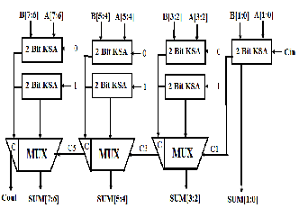
Fig. 6. Kogge Stone Based Carry Select Adder
From the above diagram it is clear that first two bit operation is done using kogge stone addition method. And all other paired block has been calculated twice by the same method assuming two different carry signal i.e. either 0 or 1. Then we need several multiplexers in order to select actual sum.
4 Results & Discussions
The above mentioned adders are implemented in Verilog HDL and their functionality has been verified in NC-Sim Tool of Cadence. After that they are synthesized using Cadence Encounter RTL Compiler. Each Adder circuit is designed for three different bit lengths i.e. 8 bit, 16 bit, and 32 bit and the performance parameters such as Timing analysis, Area and power Analysis has been obtained and shown in a tabular manner.
TABLE 1
PERFORMANCE COMPARISON TABLE FOR 8 BIT ADDERS
Name of Adders | Delay (in ns) | Area (Cell area) | Power (in mw) | Power Area product | Power delay product |
RCA | 3.71 | 1044 | 0.483 | 504.25 | 1.791 |
CLA | 3.29 | 995 | 0.583 | 580.08 | 1.915 |
CSLA | 2.79 | 1035 | 0.659 | 682.06 | 1.838 |
KSA | 2.78 | 1181 | 0.688 | 812.53 | 1.912 |
CSA | 3.09 | 965 | 0.598 | 577.07 | 1.847 |
Modified Adder | 1.76 | 1567 | 1.44 | 2256.4 | 2.53 |
TABLE 2
PERFORMANCE COMPARISON TABLE FOR 16 BIT ADDERS
Name of Adders | Delay (in ns) | Area (Cell area) | Power (in mw) | Power Area product | Power delay product |
RCA | 5.2 | 2199 | 0.711 | 1563.48 | 3.701 |
CLA | 4.1 | 2213 | 0.982 | 2173.16 | 4.026 |
CSLA | 3.76 | 2325 | 1.316 | 3059.70 | 4.948 |
KSA | 3.77 | 2162 | 1.033 | 2233.34 | 3.894 |
CSA | 4.3 | 1993 | 0.860 | 1713.98 | 3.698 |
Modified Adder | 1.82 | 3420 | 2.93 | 10020.6 | 5.332 |
TABLE 3
PERFORMANCE COMPARISON TABLE FOR 32 BIT ADDERS
Name of Adders | Delay (in ns) | Area (Cell area) | Power (in mw) | Power Area product | Power delay product |
RCA | 5.3 | 4986 | 1.524 | 7598.66 | 8.077 |
CLA | 4.69 | 4667 | 1.729 | 8069.24 | 8.109 |
CSLA | 5.29 | 4650 | 1.679 | 7807.35 | 8.882 |
KSA | 5.28 | 4514 | 1.580 | 7132.12 | 8.342 |
CSA | 5.32 | 4258 | 1.497 | 6374.22 | 7.964 |
Modified Adder | 2.39 | 7185 | 4.54 | 32619.9 | 10.85 |
From the table I, II, & III we get the different performance parameters like delay between data path, Area utilization, Total Power dissipation, Power density, Power Delay Product for comparative analysis of described adder circuits for different bit length i.e. 8 bit, 16 bit, 32 bit. From the table I we can see that except the modified Carry Select adder circuit, Kogge stone adder is the fastest (2.78 ns) among all but area utilization is more than other adders as it is one of the major disadvantage of Kogge-Stone Adder. But alternatively Carry Select adder also gives us almost same speed of operation (2.79 ns) but with a lesser Area power product and better
IJSER © 2015 http://www.ijser.org
International Journal of Scientific & Engineering Research, Volume 6, Issue 4, April-2015 921
ISSN 2229-5518
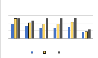
power delay product (1.838 pj). Another interesting point is in spite of having greatest delay (3.71 ns), Ripple carry adder dissipates lesser power due to its simplified architecture resulting a better Power delay product (1.791 pj).Figure 1: Block Diagram of 4 bit Ripple carry adder.
Encounter tool.
propagation Delay
6
4
2
0
RCA CLA CSLA KSA CSA Modified
8 bit 16 bit 32 bit
Fig. 7: Propagation Delays of different Adders
From the figure 7 we can easily say that apart from the basic adders the Modified Carry Select Adder is much faster and thus required lesser time to execute any addition process where as other adders like Kogge stone adder, Carry Select Adder also have very close delay value compared to Ripple carry Adder, Carry Look ahead adder and Carry Save adder.
But the there is a basically a tradeoff exits between the three basic performance parameters i.e. Delay, Power and Area utilization. If we try to improve any one of this parameter value the other two will definitely degrade. Similarly in this paper we try to modify Carry Select Adder by replacing its Ripple carry Adder block with high Speed Kogge Stone Adder, The delay inside the data path has reduced by 37% approximately (for 8 bit) whereas the area utilization and power dissipation has drastically increase. As the no of bits increase the reduction of delay also increases. For 16 bit and 32 bit operations the delay has been reduced by
52% and 55% respectively. The Modified Kogge Stone Based Carry Select Adder is very competent when the design really needs a faster speed of operation.
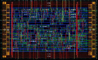
Fig. 8: RTL Schematic of 32 bit Modified Adder Circuit
The Layout of 32 bit Modified Adder Design has been generated by TSMC 180nm Standard Cell in Cadence
Fig. 9: Layout of 32 bit Modified Adder Circuit
5 Conclusion
In this paper we have compared few basic adder circuitry in terms of delay, power dissipation, area utilization etc. and then merge two of them in order to make a faster adder design. The resulting adder works significantly faster than the rest only at the cost of greater power dissipation and more area. The Modified adder which is designed in Verilog HDL and synthesized in cadence RTL Compiler has shown notable reduction of delay i.e. 37%, 52% and 55% for 8 bit, 16 bit, 32 bit of operation respectively. This work can be forge ahead in analog Transistor level in order to further minimize the delay and optimize the power also by using several low power techniques.
References
[1] Jackson.D.J and Hannah S.J “Modelling and comparison of Adder design in Verilog
HDL” IEEE Trans. on System theory, 1993 Proceeding SSST’93.
[2] Jayanthi A.N & Ravichandran “Comparison of performance of High Speed VLSI adders” IEEE conference on current Trends in Engineering and Technology (ICCTET), 2013.
[3] Maroju Saikumar & Dr.P.Samundiswary ,”Design and performance analysis of various Adders using Verilog” International journal of computer Science and Mobile Computing (IJSMC) Vol 2 issue 9 ‘2013
[4] Pallavi Saxena, Urvashi Purohit, Priyanka Joshi, “Analysis of Low Power, Area Efficient & High Speed Fast Adder” International Journal of
Advanced research on Computer and Communication Engineering, 2013. [5] Edison A.J &C.S.Manikandababu, “An Efficient carry select Architecture
for VLSI Hardware Implementation” International journal on management,
IT and Engineering, May 2012.
[6] Shivani Parmar & Kirat Pal Singh, “Design of High Speed Hybrid Cary Select
Adder” 3rd IEEE International advance computing conference (IACC), 2013.
[7] P.Chaitanya Kumari & R.nagendra, “Design of 32 bit Parallel prefix Adders” IOSR Journal of Electronics & Communication Engineering, June 2013.
IJSER © 2015 http://www.ijser.org