the intermediate hash value using the message block as key. Hence there are two main components to describe: (1) the SHA-256 compression function, and (2) the SHA-256 message schedule.
International Journal of Scientific & Engineering Research, Volume 5, Issue 7, July-2014 757
ISSN 2229-5518
Design of DDR SDRAM Controller with inbuilt
Memory Integrity Verification Module
Suvarna P, Nandakumar R.
2.
—————————— ——————————
DDR is an updated production of SDRAM. In order to achieve high-speed operation, it uses a double data rate architecture in which an interface is designed to transfer two data words per clock cycle at the I/O pins. The DDR SDRAM memory controller is used as a generic interface to the DDR SDRAM memory devices and provides a synchronous command interface to user requirements.
As DDR memory devices play the role of main memory
module in computer systems its protection is very important
and critical. In modern computer environments the operating system itself can prevent inter process access of data by memory isolation techniques. Yet inbuilt bugs within the OS can be manipulated by malicious attackers. Hence, a simple method has been suggested in this paper in order to provide an efficient memory integrity verification technique.
The SHA-2 function belonging to the family of cryptographic hash functions can be used here to verify the memory integrity.
SHA-2, though not as widely used as SHA-1 has lower collision possibility and facilitates faster and larger bit rates
than SHA-1.
The focus of this work is to develop the behavioral model of
the controller, using verilog HDL (IEEE 1364-2005). It also
gives an idea that can be realized to prevent memory
corruption. The targeted DDR SDRAM memory is Micron®
MT46V4M16 and prototyping was done in Altera® Cyclone™ II series FPGA.
SHA-2 is a set of cryptographic hash functions (SHA-224, SHA-256, SHA-384, SHA-512) designed by the U.S. National Security Agency (NSA) and published in 2001 by the NIST as a U.S. Federal Information Processing Standard. A hash function is an algorithm that transforms (hashes) an arbitrary set of data elements, such as a text file, into a single fixed length value (the hash). The computed hash value may then be used to verify the integrity of copies of the original data without providing any means to derive said original data [6].
SHA-2 consists of a set of four hash functions with digest
sizes (output size) that are 224, 256, 384 or 512 bits. SHA-256 will be suitable here as high speed data tracking is desirable. It is considered secure with no known theoretical vulnerabilities and it has a reasonable digest size of 32 bytes.
The SHA-256 operates such that the message to be hashed is first (1) padded with its length in such a way that the result is a multiple of 512 bits long, and then (2) parsed into 512-bit message blocks M(1), M(2),......., M (N). The message blocks
are processed one at a time: Beginning with a fixed initial hash value H(0) , sequentially compute
H(i) = H(i–1 ) + CM(i) (H(i–1 )) (1)
where C is the SHA-256 compression function and + means word-wise mod 232 addition. H(N) is the hash of M [8].
The SHA-256 compression function operates on a 512-bit message block and a 256- bit intermediate hash value. It is essentially a 256-bit block cipher algorithm which encrypts
IJSER © 2014 http://ww w .ij s er.org
International Journal of Scientific & Engineering Research, Volume 5, Issue 7, July-2014 758
ISSN 2229-5518
the intermediate hash value using the message block as key. Hence there are two main components to describe: (1) the SHA-256 compression function, and (2) the SHA-256 message schedule.
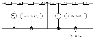
Fig. 1. jth internal step of the SHA-256 Compression function, C
In Fig. 1., it shows the jth iteration in an SHA-2 family compression function. Here, a, b, c, d, e, f, g and h are registers. Sn is right rotation by n bits, Rn is right shift by n bits. Operations performed are as follows:
Ch(e,f,g) = (e^f) xor (¬e^g)
Maj(a,b,c) = (a^b) xor (a^c) xor (b^c)
Σ0(a) = S2(a) xor S13(a) xor S22(a)
Σ1(e) = S6(e) xor S11(e) xor S25(e) σ0(a) = S7(a) xor S18(a) xor R3(a) σ1(e) = S17(e) xor S19(e) xor R10(e)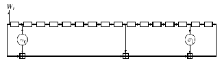
also, the symbol, ![]() denotes mod 232 addition.
denotes mod 232 addition.
Fig. 2. SHA-256 message schedule
In Fig. 2., Wj indicates expanded message blocks and can be computed by using the following equation,
Wj = Mj(i) For j = 0, 1,....., 15, and for j = 16 to 63
{
DRAM. DDR SDRAM uses the double data rate architecture to achieve high speed operation, which is essentially a 2n prefetch architecture, where n is the number of bits. The architecture contains an interface designed to transfer two data words per clock cycle at the I/O pins. A single read or write access for the DDR SDRAM consists of a single 2n bit wide, one clock cycle data transfer at the internal DRAM core and two corresponding n bit wide, one half clock cycle data transfers at the I/O pins. Read and write accesses to the DDR SDRAM are burst oriented. Programmable READ or WRITE burst lengths of 2, 4, or 8 locations can be provided. At the end of every burst access a self timed row precharge will be initiated using an auto precharge function. Prior to normal operation, the DDR SDRAM must be powered up and initialized [4].
The Micron® 64Mb [5] DDR SDRAM referenced in this paper is a high – speed CMOS, dynamic random access memory containing 67,108,864 bits. It is internally configured as a quad – bank DRAM. Each of the 16,777,216 bit banks are organized as 4,096 rows by 128 columns by 32 bits. All inputs are compatible with the JEDEC Standard for SSTL_2. All full drive outputs are SSTL_2, Class II compatible.
The pin diagram for the controller is shown in Fig. 3.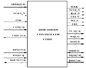
Wj σ1(Wj–2) + Wj–7 + σ0(Wj–15) + Wj–16 (2)
}
The registers in Fig. 2. are loaded with W0, W1,........, W15
The DDR SDRAM targeted is a high speed CMOS, dynamic random access memory internally configured as a quad bank
Fig. 3. Pin Diagram - DDR SDRAM Controller
The inputs to the controller are fed by the user and the outputs from the controller are fed to the memory inputs.
The signal name, type and description of each signal is given
in Table I [9].
IJSER © 2014 http://ww w .ij s er.org
International Journal of Scientific & Engineering Research, Volume 5, Issue 7, July-2014 759
ISSN 2229-5518
TABLE I
PIN DESCRIPTION – DDR SDRAM CONTROLLER
The DDR SDRAM controller [9] is designed to provide a simplified interface to the industry standard DDR SDRAM memory Micron® MT46V4M16. It has a user interface at one side and the memory at the other side. Burst lengths of 2, 4 or
8 and CAS latencies of 1.5, 2.0, 2.5 or 3.0 can be programmed
using the controller. Data mask lines are supported for
WRITE operations. The controller supports seven commands including two for the load registers.
The commands are: NOP, READ, WRITE, REFRESH, PRECHARGE and LOAD_REG. Data mask lines are supported for WRITE operations. It supports the following commands: NOP, READ, WRITE, REFRESH, PRECHARGE
and LOAD_REG. Data path widths of 16, 32 and 64 bits are possible. It uses two different frequency, 100 MHz and
200MHz output clocks to facilitate enhanced performance. The DDR SDRAM is controlled by bus commands that are formed using combinations of RAS_N, CAS_N and WE_N
signals.
output clocks of 100MHz and 200MHz each and a locked clock output to improve I/O timing. The control and interface modules decodes the NOP, READ, WRITE, PRECHARGE,
The detailed architecture of the proposed controller is shown in Fig. 4. DDR SDRAM Controller module consists of three main modules, the Control Interface, Command and Data Path Modules. The DDR SDRAM Controller module is the top-level module that instantiates the three lower modules and brings the whole design together. The inputs to the controller are fed by the user and the outputs from the controller are fed to the memory inputs. The Control Interface module accepts commands and related memory addresses from the host, decoding the command and passing the request to the Command module. The command module accepts command and address from the Control Interface Module, generating the proper commands to the SDRAM. The data Path Modules handles the data path operations during WRITE and READ commands [9]. The top-level module also instantiates a PLL that is used to generate two
REFRESH and LOAD_REG commands and passes them along with ADDR to the command module.
IJSER © 2014 http://ww w .ij s er.org
International Journal of Scientific & Engineering Research, Volume 5, Issue 7, July-2014 760
ISSN 2229-5518
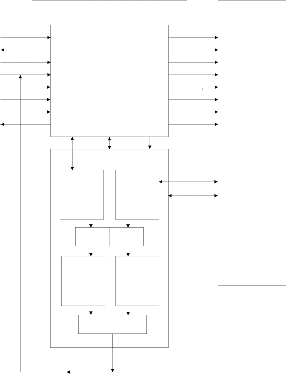

the data within each block have to be transferred to the SHA engine where the hash functions are used to perform equal operations on both the data. For every READ operation the data stored in the original data hash table during the previous WRITE command should match that of the untrusted data hash table. Also during the WRITE command the column data specified in the address line saddr[11:0] will be written to both the trusted and untrusted blocks. This data after performing hash operations within the SHA engine and stored in the data hash tables should also match each other. If a match occurs it indicates that the memory is not corrupted and so a logic HIGH is generated by the hash function comparator. Otherwise a logic LOW is forced on to the RESET_N pin which helps to flush the corrupted data from the memory. During the next command cycle a NOP command issued by the controller again brings back the RESET_N pin HIGH to facilitate further memory transfers.
DDR SDRAM CONTROLLER CORE
CLK CMD_ACK ADDR[21:0]
RESET_N
CMD[2:0] DM[15:0] DIN[127:0] DOUT[127:0]
MEMORY CONTROL LOGIC
dq[63:0] dqs[7:0] saddr[21:0]
INTEGRITY VERIFICATION ALGORITHM
CAS_N RAS_N WE_N
CKE CS_N[1:0] SA[11:0] BA[1:0] DQM[7:0]
DQ[63:0]
DDR SDRAM MEMORY MODULE (Vulnerable to Corruption – Un-trusted)
ORIGINAL DATA
UN-TRUSTED DATA
DQS[7:0]
SHA ENGINE
text
Fig. 4. Detailed Architecture – DDR SDRAM Control Logic
Refresh commands also are periodically registered to the
HASH FUNCTION TABLE I ORIGINAL DATA
HASH FUNCTION TABLE II
UN-TRUSTED DATA
command module using this module. The command module generates appropriate signals to the memory by accepting decoded commands from the control and interface module. It also contains a bus arbiter that arbitrates between the commands from the host interface and the refresh requests from the refresh control logic. The data path width in to the controller is two times the width to the DDR SDRAM device. DIN and DOUT are fixed at 32 bits and the DQ port is fixed at
16 bits. Data path modules can be cascaded to increase the
data bus width in increments of 32 bits as shown in Fig. 4.
The integrity verification algorithm is illustrated in Fig. 5.
As shown in the figure, there are two blocks which can be DQ sized arrays used to store the original data and the possibly untrusted data. DQS[7:0], dqs[7:0] and saddr[11:0] is used to sync the appropriate data storage within these blocks. Then
HASH FUNCTION
COMPARATOR
(1/0) Verified Integrity Information
Fig. 5. DDR SDRAM Controller Core with Memory Integrity Verification
Algorithm
The architectural design was tested by using a test bench with test signals as shown in Fig. 9. A set of preferable input combinations were forced to act upon the controller inputs so that correct results were obtained as waveforms. The simulated results were obtained in ModelSim® by applying appropriate delay elements.
IJSER © 2014 http://ww w .ij s er.org
International Journal of Scientific & Engineering Research, Volume 5, Issue 7, July-2014 761
ISSN 2229-5518
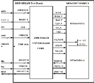
Fig. 6. Test Bench – DDR SDRAM Controller Core
The design was synthesized by porting to Altera® Cyclone™ II - EP2C20F484C7 FPGA and results were verified using SignalTap® II Logic Analyzer tool in Altera Quartus® II software.
This paper describes the architecture design of DDR SDRAM Controller IP Core with an inbuilt memory integrity verification module. The proposed architecture can successfully control the different commands to the DDR SDRAM memory module. The design was modeled using verilog HDL and can be easily adapted for several different design requirements. The paper also suggests a modest, yet efficient method to protect the memory from being corrupted while transfer of data between the memory and other modules. Even though DDR SDRAMs higher generations are available now, a DDR SDRAM memory was used here as its standards are still being deployed and improved. This method for memory integrity verification if realized can be applied to DDR2 and also higher generations of memory devices.
REFERENCES
[1] Micron 1GB DDR SDRAM datasheet, Micro Technology
Inc. 2003.
[2] How to use DDR SDRAM, Elpida Memory, Inc. 2002.
[3] Micron Technology Inc., "DDR SDRAM Functionality and Controller Read Data Capture", Design Line, Vol.8, Issue 3, Sep. 1999.
[4] JEDEC. Double Data Rate (DDR) SDRAM Specification.
JEDEC Solid State Technology Association, JESD79F
edition, May 2005.
[5] Micron Technology Inc., “DDR SDRAM: MT46V4M16D1TG-7 Data Sheet”.
[6] https://en.wikipedia.org/wiki/SHA-2
[7] Weidong Shi .“Architectural Support for Protecting
Memory Integrity and Con¯dentiality”, College of
Computing Georgia Institute of Technology August 2006. [8] “Descriptions of SHA-256, SHA-384, and SHA-512”, http://csrc.nist.gov/groups/STM/cavp/documents/shs
/sha256-384-512.pdf
[9] “An Improved Memory Integrity Protection Scheme”,
February 21, 2010.
[10] Atsuya Okazaki “Efficient Off-chip Memory Integrity Verification for Secure Processor”, Graduate School of Information Science, Nara Institute of Science and Technology, February 2005.
[11] G. Edward Suh, Dwaine Clarke, Blaise Gassend, Marten
van Dijk, Srinivas Devadas “Efficient Memory Integrity Verification and Encryption for Secure Processors”, MIT Computer Science and Artificial Intelligence Laboratory Cambridge, MA 02139, USA 2003
[12] Yin Hu “An Efficient Scheme to Provide Real-time
Memory Integrity Protection”, Worcester Polytechnic
Institute, May 2009.
[13] A. C. Bonatto, A. B. Soares, A. A. Susin. “DDR SDRAM
controller IP designed for reuse,” In: IP Based Electronic
System Conference & Exhibition - IP 08, France. Design
and Reuse, pp. 175-180, 2008.
[14] Thomas, Donald, Moorby, Phillip "The Verilog Hardware Description Language" Kluwer Academic Publishers, Norwell, MA.
[15] ALTERA, DDR SDRAM Controller White Paper, Ver1.1,
2002, 8.
[16] DDR SDRAM Controller, Reference Design RD1020, Lattice, Semiconductor Corporation, April 2004.
жжж
IJSER © 2014 http://ww w .ij s er.org