circuit description is presented. Section III presents circuit analysis units. In the section V, we demonstrated
simulation result. The results were obtained by simulation
produce in a 0.35 µm processions form the last section.
International Journal of Scientific & Engineering Research, Volume 4, Issue 7, July-2013 925
ISSN 2229-5518
Design of A Programmable Bandgap Reference
Circuit
Khadijeh Karamzadeh, Akaram Asghari Govar, Jafar Sobhi, Hamid Moharrami
feedback mode, and it generates its own reference current, resulting in a stable operation. A startup circuit is required for successful operation of the system.
Index Terms—Proportional To Absolute Temperature (PTAT), Conversely proportional To Absolute Temperature (CTAT), BandgapReferenc
(BGR), Temperature Coefficient (TC).
————————————————————
A KEY ELEMENT of analog-to-digital (A/D) and digital- to-analog (D/A) converters is a precise voltage reference with good temperature stability. Accurate biasing voltages are critical for many circuit schemes; in ADC, a reference voltage is required to quantify an input, while in DAC, it is required to define the output full-scale range. As a well- established reference generator technique, bandgap reference is most popular for both Bipolar and CMOS technologies.
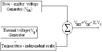
The principle of the bandgap circuits relies on two groups of diode-connected BJT transistors running at different emitter current densities. By canceling the negative temperature dependence of the PN junctions in one group of transistors with the positive temperature dependence from a PTAT (proportional-to-absolute- temperature) circuit which includes the other group of transistors, a fixed DC voltage which doesn’t change with temperature is generated.[3][4] There are many different implementation reported, while essentially a bandgap reference circuit consists of a supply independent biasing circuit, a diode connected BJT transistor generating a voltage with negative temperature coefficient, a PTAT circuit and some kind of feedback mechanism to improve the performance. This working principle of a bandgap voltage reference can be illustrated by Fig1 since VRBER decreases approximately linear with temperature while VRTR increases linearly with temperature, a low-temperature- dependence VRREFR can be obtained by scaling up VRTR and summing it with VRBER.
The outline of this paper is as follows: in section II
————————————————
• KhadijehKaramzadeh, Electrical Dept.,Eng.Faculty,Islamic Azad
University,MiyanehBranch,Miyaneh,Iran,kh_karamzadeh_h@yahoo.com
• AkaramAsghariGovar, Electrical Dept.,Eng.Faculty,Islamic Azad
University,AharBranch,Ahar,Iran, asghari.akram@gmail.com
• Jafar Sobhi, Electrical Dept.,Eng.Faculty, university of Tabriz,
Tabriz,Iran,sobhi@tabrizu.ac.ir
• HamidMoharrami, Electrical Dept.,Eng.Faculty,Islamic Azad
University,MiyanehBranch,Miyaneh,Iran,h_moharrami_kh@yahoo.com
circuit description is presented. Section III presents circuit analysis units. In the section V, we demonstrated
simulation result. The results were obtained by simulation
produce in a 0.35 µm processions form the last section.
Fig. 1.Concept of bandgapVoltage Reference
Adding two voltages that have temperature coefficients of opposite sign with suitable multiplication constants generates a reference voltage. The resulting voltageobtained is independent of temperature. The diode voltagedrop across the base-emitter junction, VBE, of a BipolarJunction Transistor (BJT) changes Complementary toAbsolute Temperature (CTAT) [1]. Whereas if two BJTsoperate with unequal current densities, then the difference inthe base emitter voltages, ∆VBE, of the transistors is found tobe Proportional to Absolute Temperature (PTAT). The PTATrelationship is given by [2],
∆VBE = VT ln m; VT = kT /q (1)
where, k is Boltzmann’s constant, T is the absolutetemperature, q is the electron charge and m is the ratio of thecurrent densities of the two BJTs. The PTAT voltage may beadded to the CTAT voltage with suitable
IJSER © 2013 http://www.ijser.org
International Journal of Scientific & Engineering Research, Volume 4, Issue 7, July-2013 926
ISSN 2229-5518
weighting constantsto obtain a constant reference voltage.
It should be noted that in this section Rx is neglected. Fig.3 shows the block diagram of the variable badgap
times thecurrent density of the m BJTs identical to A, connected inparallel. The voltages at node X and Y are maintained at thesame value, VBE using a feedback network through adifferential amplifier. The voltages VBE and ∆VBE are addedtoobtain the reference voltage. The circuit also requires a startup circuit since there exists a stable state at which no current flows through the circuit. The startup circuit forces the transistors to turn on and the circuit to operate at its other stable state to generate the reference voltage.
referencecircuit designed. By using a supply independent currentsource, a current ISS is passed through BJT A. The samecurrent ISS flows through m transistors connected in parallel,identical to A. Thus the current density of A is m
Fig 4: Schematic of Bandgap Reference Circuit showing the supply independent current source and generation of reference
voltage.
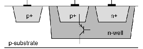
It should be noted that an ideal BJT is not available in CMOS technology. A pnp BJT is made using the n-well normally associated with a PFET [1] the p-substrate behaving as the collector.
In order to generate supply independent current and carry
out an addition of the CTAT and PTAT voltages, the circuit
in Fig4 is used. The OPAMP provides the base voltage to the transistors, which are connected as current mirrors. By
selecting the value of R1 and current ISS, the circuit may be designed to operate at the desired operating point. The value of R1 is given by,
R1 = ∆VBE / I SS (2)
Since the same current ISS flows through R2, the voltage at the output reference voltage nodes is given by,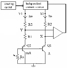
Vref
= VBE + I SS R2
V = V
+ ∆V
![]()
. R2 = V
![]()
+ R2 .V
. ln m (3)
Fig. 2. Block diagram of Bandgap Reference Circuit.
ref BE
BE BE T
1 1
Fig. 3 .pnp BJT using CMOS process.
Thus by selecting the value of R2 the weighting constant may be set. This arrangement provided an elegant arrangement to generate the reference voltage while conserving voltage headroom. The circuit has a stable operating point at which no current to flows through it. An arrangement must be made to force the saturation when the supply is turned on. The startup circuit carries out this function.
The bandgap reference voltage is generated by adding the base emitter voltage, VBE, of a BJT to the difference in base emitter voltage, ∆VBE of BJTs with a ratio of current density m. In order to generate a stable circuit, it is necessary to keep the BJT in the exponential region.
The change of the voltage of reference node is made possible by adding variable resistor in the base of Q1 and Q2 transistors. This method supplies the acceptable thermal characteristic to some extent (Fig4).
Ideally, the error amplifier has a high voltage gain A, and therefore VRXR=VRYR can be achieved, when R2=R3,
IJSER © 2013 http://www.ijser.org
International Journal of Scientific & Engineering Research, Volume 4, Issue 7, July-2013 927
ISSN 2229-5518
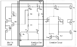
VDSTP1 =VDSTP2 can be easily obtained to provide a very good current matching by TP1 and TP2. VREF can be generated by this structure without the need of an extra current branch. Both power consumption and errors can be reduced effectively.
The voltages X and Y are fixed by feedback, hence result the VREF is given
I SS
before. Therefore only R2 and Rx are affected in the thermal characteristic. If R2 is much more than Rx/β, effect of the Rx in thermal characteristic would be neglected.
The OPAMP was used to maintain equal node voltages and provide a feedback to maintain the drain currents constant and insensitive to supply variations. A high gain of the OPAMP would result in better voltage tracking of nodes X![]()
Vref
= VBE + I SS .R2 +
β .Rx (4 )
and Y
(Fig4). The common mode voltages play an important role in determining the OPAMP topology. The input
V = V + I
![]()
R + Rx
(5)
common mode was determined by the base emitter voltage
ref
BE SS ( 2 β )
of the BJT, which is 0.8 V at 100 μA of collector current. In order to meet the input common mode condition an active
Vref
= VBE
![]()
+ ∆VBE
(R2
![]()
+ Rx )
(6)
current mirror circuit with a PMOS driver was selected.
R1 β
The output common mode voltage corresponds to the gate voltage of the current mirror transistors. In order to have a VDSAT of 0.4 V for these transistors the output
common mode should be ideally about 1.5 V. A second stage
Vref
= VBE
![]()
+ ( R2 +
R1
![]()
Rx
βR1
).VT
. ln m
(7)
was added to the OPAMP to increase gain and shift the common mode voltage up by using an NMOS driver. The
In the order achieve a zero temperature coefficient; the following equation must be satisfied.
NMOS driver only provided an output common mode of about 0.4 V. By adding a diode-connected transistor, TN7, to the second stage, the output voltage was pushed up to about
1.3 V without any effect on the gain of the stage. The voltage drop accress the diode connected transistor is about 1.2 V
∂Vref
![]()
∂T
![]()
= ( R2 +
R1
Rx
![]()
β .R1
![]()
) ln m. ∂VT
∂T
![]()
+ ∂VBE
∂T
(8)
corresponding to VTH + VDSAT. The gain of each of the stages of the OPAMP is given by
A=gm.Ro (11)![]()
∂Vref = 0
∂T
(9)
Where, Av is the gain, gm is the transconductance of the driving transistor and RO is the effective output resistance at the output node.![]()
⇒ ( R2 +
R1
(10)
Rx
![]()
β .R1
![]()
) ln m. ∂VT
∂T
![]()
= − ∂VBE
∂T
Transistors TN1, TN2, TN3 and TP4 constitute the startup circuit. Initially all the transistors start off in off state. The voltage at the gate of TN1 is low and so it remains in off
The equation shows that R1, R2, Rx and m affect on the TC of Vref. m is the ratio of the surface of Q1 and Q2 transistors. Because layouts on both BJTs and resistors should be well planned and designed so that consistent performance can be maintained with minimum need of trimming in mass productions. Better matching can be achieved by a common-centroid layout [6],[7]. However a large value of N is not preferred as the separation of devices increases, and this will introduce more errors. Moreover, as shown in (1) there is no signification increase on the ln(m) function when m increases.
For the resistor layout, common-centroid layout should be also used to obtain better matching[7]. Polysilicon is a better material than diffusion since its tempco is low. An even better material is high-resistive polysilicon, since it has a negative tempco. We used in the simulation.
As mentioned above, the amplitude of R1 and m are set
state. TP4 being diode connected is always on and so the transistor TN2 turns on forcing the drain to a low value. The current mirror stack turns on and the gate voltage of TN1 rises and it starts to conduct. At this point there is a competition between the output of the amplifier TP6, and TN2 for the current source load. TN2 is designed to be a weak transistor so the amplifier takes control of the current mirror gate.
When the bandgap voltage is high enough ( ~1V) the transistor TN1 turns on. TN1 in linear region has to compete with TN2 in saturation so it is designed to be a big transistor. It draws all the current from TP2 and the base voltage of TN2 falls till it turns off. In this state the gate voltage at TN2 is about 0.6 V. This is high enough for the transistor TN1 to be conduct slightly. A diode connected transistor TN3 is added to increase the threshold voltage at the gate of TN3 to turn off. The transistor TP4 is designed to be a weak device
IJSER © 2013 http://www.ijser.org
International Journal of Scientific & Engineering Research, Volume 4, Issue 7, July-2013 928
ISSN 2229-5518
so that low current flows through the parasitic path when the circuit is in full operation.
The variable bandgap reference voltage gives a voltage of
1.2672V when adjusted to have a zero temperature
coefficient at 27C when RX is 900Ω. Fig5 shows the result of
the simulation. As can be seen an overall temperature coefficient of 0.0141mV/K is obtained between 0C and 85C,
which corresponds to about 0.0946% variation. The response it worse for temperatures from 64-85˚C with a temperature coefficient of 0.0571mV/K. Below these temperatures the temperature coefficient is 0.01875mV/K.
Fig 6 shows the variation Vref when the Rx is varied
from 1Ω to 2.4kΩ. The relative variation Vref is 2.79mv/kΩ
1.313
1.312
1.311
1.31
1.309
1.308
1.307
1.306
1.305
1.304
1.303

0 5 10 15 20 25 30 35 40 45 50 55 60 65 70 75 80
Temperature (c)
at 27˚C. So the worst case operation of the device is when Rx is 2.4kΩ and 1Ω. In the table1, PSRR and TC are shown for different Rx.
Fig 7 shows variation of Vref when temperature changes between 0˚C to 80˚C. Temperature coefficient of 0.1mV/K is obtained.
The D.C characteristics at 80 degrees are shown in Fig 8. The variation with Vdd is much worse in this case. The simulation demonstrated PSRR is 37dB.
1.2678
1.2676
1.2674
Fig7 .Variation of bandgap reference with temperature at
Vdd=3.3V and Rx=2400Ω
1.2678
1.2677
1.2676
1.2675
1.2674
1.2673
1.2672
1.2671
1.267
1.2669
1.2668
1.2672
1.267
1.2667
3 3.1 3.2 3.3 3.4 3.5 3.6
VDD (volt)
1.2668
Fig8: Variation of the reference voltage with supply voltage at 27C
1.2666
1.2664
1.2662
0 5 10 15 20 25 30 35 40 45 50 55 60 65 70 75 80 85

1.268
1.2678
1.2676
1.2674
Fig5 .Variation of bandTgemapperartueref(ce)rence with temperature at
Vdd=3.3V and Rx=900Ω

1.305
1.295
1.285
1.2672
1.267
1.2668
1.2666
1.2664
1.275
1.265
1.2662
3 3.1 3.2 3.3 3.4 3.5 3.6
VDD (volt)
1.255
Fig 9: Variation with Supply Voltage at 80 C (absolute worst case)
1.245
1.235
0 10 20 30 40 50 60 70 80
Temperature (c)
TABLE 1
REFERENCE VOLTAGE OBTAINED UNDER DIFFERENT RX
Fig6 .Variation of bandgap reference with temperature for
Rx=1Ω to 2.4KΩ (Vdd=3.3V )
IJSER © 2013 http://www.ijser.org
International Journal of Scientific & Engineering Research, Volume 4, Issue 7, July-2013 929
ISSN 2229-5518
TABLE 2
SUMMARY OF PERFORMANCE W ITH AND WITHOUT RX
[7] D. John and K. Martin ,“Analog Integrated Circuit Design”, Wiley 1997.
[8] Hasting, “The art of Analog Layout Englewood Cliffs”, NJ: Prentice-Hall,
2001.
This circuit is simulated for FF, SS, FS and SF model. PSRR for FF, FS, SF and SS corner was 52dB, 55dB, 56dB and
60db and TC also was 15, 10, 50, and 20 ppm/C. These results show that FS is worse case for this circuit.
A bandgap reference with a current feedback mode has been designed. The circuit uses no external current sources and is designed to have a zero temperature coefficient at 27˚C. The design is simulated implemented with 0.35µm CMOS process. The circuit generates a variable reference voltage of
1.2380 until 1.3051. Table 2 shows the summary of
performance of proposed circuit. The output voltage is
1.2659V at the nominal operating condition of 27˚C
temperature and 3.3V supply voltage. It has a temperature coefficient of 0.0141mV/K from 0-804˚C.
[1] B. Razavi,” Design of Analog CMOS Integrated Circuits”, New york, NY:
2001, ch 11.
[2] D. Hilbiber, “A New Semiconductor Voltage Standard”, IEEE J. of Solid-State
Circuits, vol. 8, pp. 222-226, June 1973.
[3] Robert A. Pease, “The Design of Band-Gap Reference Circuits: Trials and Tribulations”, IEEE Proc. of the 1990 Bipolar Circuits and Technology Meeting, Minneapolis, Minnesota , Sept. 1990.
[4] K. Lasanen, V. Koorkala, etc., “Design of A 1-V Low Power CMOS Bandgap
Reference Based on Resistive Subdivision”, IEEE 2002
[5] T. Brooks and A.C Westwisk, “ A low power differential CMOS bandgap
Reference”, ISSCC Dig.Of Tech. Papers, pp 248-249, Feb 1994.
[6] K. Lasanen, et. Al, “ Design of a 1-V low power bandgap reference based on Resistive Subdivision”, Proceedings of the 45th IEEE Midwest Symposium on Circuits and Systems, Tulsa, Oklahoma, USA, August 2002.
IJSER © 2013 http://www.ijser.org