International Journal of Scientific & Engineering Research Volume 3, Issue 4, April -2012 1
ISSN 2229-5518
Design and development of a C-Band frequency up-converter system
Anupam Bhardwaj, G.Boopalan, Pinaki Sen, Nupur Sood
Abstract: In this paper a broadband up-converter system has been designed and realized using ADS simulation and designing tool. It is a Radio Frequency transmitter block up-converting the Input Frequency in two stages to reach to the desired frequency level and then transmit it to the antenna port. It contains of oscillators, amplifiers, step attenuators, isolators, filters, and mixer blocks. The input frequ ency (IF) band is (100 + 10) MHz and the output frequency band (RF) is (5500 + 100) MHz. The attenuators are us ed to increase the dynamic range of the circuit. It is a two stage up- conversion circuit i.e. mixing the IF band at two stages to give the specified RF range. Here two phase locked oscillators ar e used at the LO port of the mixers, one giving a single frequency and the other one is a programmable frequency synthesizer providing 10 equally spaced frequency channels within S-Band. The frequency synthesizers are designed and simulated using ADS tool and loop filter components are realized using the MATLAB tool.
Key Words: Broadband, phase locked loop, frequency synthesizers, voltage controlled oscillators, mixer conversion loss, frequency divide r.
——————————————————— ———————————————————
1. INTRODUCTION
In this paper, a C-Band frequency up-converter has been
designed and simulated with help of Advanced Design
Software (ADS) tool. It is a Radio Frequency transmitter block up-converting the Input Frequency in two stages to reach to the desired frequency level and then transmit it to the antenna port. It contains of oscillators, amplifiers, step attenuators, isolators, filters, and mixer blocks.
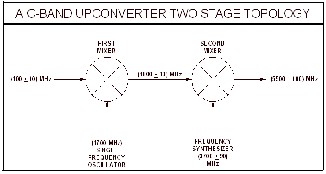
Figure 1 : Frequency Changes in Two Stages Up-converter Block
The input frequency (IF) band is 100 MHz and the output frequency band at radio frequency (RF) is 5500 MHz. The input signal is amplified and converted from 100 MHz to
5500 MHz. The attenuators and amplifiers are used to
increase the dynamic range and gain adjustments of the circuit. In this paper, the up-converter selects either of the
——————————————————————
 Anupam Bhardwaj is currently pursuing masters degree program in Communication engineering in V.I.T University, Vellore, Tamil Nadu, India, Mob: +919027884587. E-mail: anu.bhardwaj1@gmail.com
 G.Boopalan is currently working as Sr. Assistant Professor in VIT University, Vellore, Tamil Nadu, India. E-mail: boopalan@vit.ac.in
 Pinaki Sen is currently working in DEAL-DRDO, Dehradun as Scientist-F in the Microwave Division.
 Nupur Sood is currently working in DEAL-DRDO, Dehradun as Scientist-B in the Microwave Division.
dual Payload IF signal input in the frequency band of 100
MHz using a SPDT switch and then up-converts it to the
1st IF using a double-balanced mixer driven by a 1700
MHz Phase Locked Oscillator. The 1st IF is then band-
limited to 1800 MHz using a band-pass filter, before being applied to the second mixer, whose Local oscillator is realized through a programmable frequency synthesizer at 3700 MHz, tunable in fixed step size so as to provide 10 channels. The final signal in the band of
5500 MHz is then filtered and suitably amplified before being made available on the front panel of the RF Transceiver. This Frequency synthesizer at the second stage mixing is a phase locked oscillator circuit giving 10 frequency channels with fixed channel spacing at 3700
MHz.

Figure 2 : C-Band Up-Converter Block diagram
This frequency synthesizer circuit consists of a reference oscillator, a reference frequency divider (R=1), a phase/frequency detector with a charge pump, a passive low pass higher order filter, a voltage controlled oscillator and a linear VCO frequency divider.
http://www.ijser.org
IJSER © 20 12
International Journal of Scientific & Engineering Research Volume 3, Issue 4, April -2012 2
ISSN 2229-5518
In this paper, basically two design iterations are employed with the difference in the second iteration is the presence of the programmable frequency synthesizer
rather than a simple oscillator giving 10 channels as used in the first iteration. Also in the second iteration minor changes in the parameters of the various components are done to get a better output level and better level of up- conversion. And hence both the design iterations are compared on the basis of output power level, level of mixing of the signal and difference of level at required frequency and spur offset frequency.
2. SPECIFICATIONS
The block diagram and target specification for the up-
converter is shown below. Two design iterations were


performed. During the second iteration, minor changes are done and a frequency synthesizer circuit is added in the place of simple 10 channel generating oscillator at the input to second mixer as in the first iteration.
PARAMETERS | SPECIFICATIONS REQUIRED |
Input | - Frequency Band - Power Level | (100 + 10) MHz (0 + 2) dBm nominal |
Output | - Frequency Band - Power Level | (5500 + 100) MHz (0 + 2) dBm nominal |
Output RF channel selection | Through frequency synthesizer programming via M&C port |
Spurious Response | ≤ -100 dBc/Hz within the output RF band |
Frequency Synthesizer for Second Mixer | - Output - Number of channels - Channel Spacing - Phase Noise | (3700 + 90) MHz 10 (Ch:1-3610 MHz; Ch:10-3790 MHz) 20 MHz ≤ -75 dBc/Hz at 1 kHz offset ≤ -100 dBc/Hz at 10 kHz offset ≤ -120 dBc/Hz at 100 kHz offset |

3. VARIOUS SUBCIRCUITS
AMPLIFIERS:-
There are three amplifiers are used in the up-converter circuitry. Two of these amplifiers are used in the up- converter chain itself while one is used in the frequency synthesizer output. These amplifiers, Amp1 and Amp3, used in the up-converter are providing gain of 19dB and
15dB respectively.
Figure 3 : Amplifier Topology used
While the one, Amp2, used at the frequency synthesizer
output is giving gain of 12dB. Here, the schematic used for getting the required gain is shown. To improve input matching and stability, an inductor was added on the
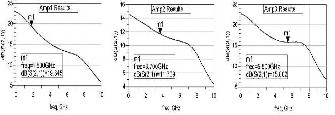
source of the first stage. The inter-stage matching network is simply a capacitor for DC isolation. Using an inductor in the feedback loop for the second stage increased the gain at the higher end of the frequency band. To improve input matching and stability, an inductor was added on the source of the first stage. The inter-stage matching network is simply a capacitor for DC isolation. Using an inductor in the feedback loop for the second stage increased the gain at the higher end of the frequency band.
Figure 4 : Respective results for the Amplifiers
ATTENUATORS:-
The attenuator block was realized by a double pi- attenuator. It consists of lumped elements resistors, inductors and capacitors. Here inductors and capacitors are used at the input and output ports for coupling while the resistors R1 and R2 are responsible to give attenuation values.
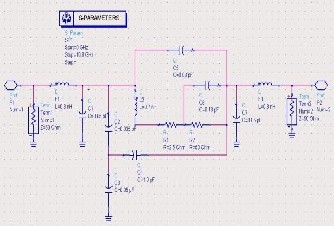
Figure 5 : Attenuator circuitry in ADS
http://www.ijser.org
IJSER © 20 12
International Journal of Scientific & Engineering Research Volume 3, Issue 4, April -2012 3
ISSN 2229-5518
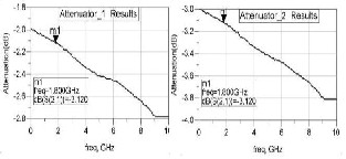
Figure 6 : Attenuation results in ADS
The attenuation of 2dB and 3dB are required here to increase the dynamic range of the up-converter. These attenuators circuits used here are Pi-pad attenuators and the attenuation is depending upon the resistors values.
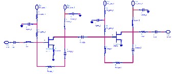
MIXERS:-
Here two single balanced diode mixers are used in the
two stage up-converter topology. The first mixer is used
to up-convert the input of (100 + 10) MHz to (1800 + 10) MHz using 1700 MHz at its LO input. It provides a conversion loss of 6 dB and it needs a LO power level to be 10dBm. The second mixer is used for up-converting the input of (1800 + 10) MHz to the required RF output (5000 + 100) MHz using the frequency synthesizer giving (3700 + 90) MHz at the LO input of the second mixer. It provides a conversion loss of 6 dB and it needs a LO power level to be 10dBm.
FREQUENCY SYNTHESIZER:-
There is a frequency synthesizer employed at the LO input of the second mixer. The frequency synthesizer has the following specifications. This frequency synthesizer is based on the concept of phase locked oscillator (PLO). Phase – locked – loop (PLL) is a feedback system used to lock the output frequency and phase to the frequency and phase of input. It can also be used as a frequency synthesizer for modulation and demodulation. Normally, PLL is used in both transmitting and receiving terminals for any wireless communication. It is composed of several components, which are phase detector, filter, voltage controlled oscillator and main divider. It operates as a negative feedback loop. While the voltage controlled oscillator generates an output signal, its output phase is fed and compared to the reference signal. This process continues until no phase difference exists. At this state, PLL is called “frequency locked”. Noise in PLL is classified into two categories, which are amplitude noise and phase noise. Amplitude noise is detected and terminated easily. In contrast, phase noise is difficult to identify and express in an equation due to unpredictable characteristics of electronic components. It affects the system performance and the signal to noise ratio.
Moreover, the benefit of having a more reliable phase noise model deals mainly with the design problem. Here, in the PLO block diagram firstly there is a crystal oscillator giving a reference frequency (Fref) followed by a reference frequency divider(R). This is one of the inputs
to the phase frequency detector having another input as the VCO output (Fout) divided by the VCO divider (N). The basic need for the phase frequency detector to work is that both the inputs should be at same frequencies


This phase frequency detector works as charge pumps i.e. phase detector (or comparator) is used to convert the phase error (i.e. the phase difference between the two inputs of the phase frequency detector) into the equivalent current (Icp) and K is referred to as charge pump gain constant.
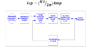
Figure 7 : PLO Block Diagram
PARAMETER | SPECIFICATION REQUIRED |
Output Frequency Range | (3700  90) MHz 90) MHz |
Step Size | 20 MHz (10 channels, Ch 1: 3610 MHz – Ch 10 : 3790 MHz) |
Output Power level | +7 dBm |
Input Reference - Frequency - Level - Stability | 10 MHz sine-wave -1 to -10 dBm 0.01 ppm |
Phase Noise | ≤ -75 dBc/Hz at 1 kHz offset ≤ -80 dBc/Hz at 10 kHz offset ≤ -100 dBc/Hz at 100 kHz offset |
Power Supply | +3.3V DC, 156 mA |
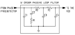

The problem that comes with the designing of the fourth- order loop filter is maintaining the required loop natural frequency (ωn) and phase margin (PM) when adding the extra attenuation.
http://www.ijser.org
IJSER © 20 12
International Journal of Scientific & Engineering Research Volume 3, Issue 4, April -2012 4
ISSN 2229-5518
Figure 8 : Loop Filter used
Within this Section a new set of formulas are presented for the exact calculation of all the fourth-order time constants, which guarantee the specified loop phase and gain margins in a PLL. This is achieved by focusing on the behavior of the transfer functions only at the specified loop natural frequency. The loop filter used in the frequency synthesizer circuitry is shown below. This loop filter is a passive fourth order low pass filter which is used for locking the frequency to the required state and providing the required level of attenuation for the spurious responses. Increasingly often a fourth-order loop filter design is used to improve the first reference spur attenuation by adding another RC pole.
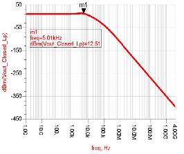
Figure 9 : Closed Loop Frequency response

Figure 10 : Phase noise variation for the frequency synthesizer
The specified attenuation frequency could equally be required at another frequency offset, to reduce other known spurious products within the synthesizer architecture. For this analysis, the required attenuation is assumed to be at the first sampling frequency spur offset, from the carrier. The frequency responses for the open and closed loop are obtained for the phase locked loop using MATLAB tool and shown below. The loop filter transfer function is represented as

;
The phase margin will be given as:
 ;
;
The time constants are calculated as:

;  ;
; 

; 
T(3,1) and T(4,1) are time constant ratios generally of the order of  or
or  . Now the loop filter components are calculated using the time constants, natural frequency (ωn), phase margin, charge pump gain constant (KΦ), VCO gain constant (Kv) and the VCO divider (N) value.

; C ;
;  ;
;

The output phase noise has been calculated and obtained using the ADS tool for the above calculated loop filter components.
4. SIMULATION RESULTS
Here, the two iterations are followed in order to receive the output at the desired radio frequency. In this paper, basically two design iterations are employed with the difference in the second iteration is the presence of the programmable frequency synthesizer at the LO port of the second mixer rather than a simple oscillator giving 10 channels as used in the first iteration. Also in the second iteration minor changes in the parameters of the various components are done to get a better output level and better level of up-conversion. And hence both the design iterations are compared on the basis of output power level, level of mixing of the signal and difference of level at required frequency and spur offset frequency.
http://www.ijser.org
IJSER © 20 12
International Journal of Scientific & Engineering Research Volume 3, Issue 4, April -2012 5
ISSN 2229-5518
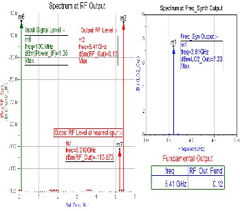
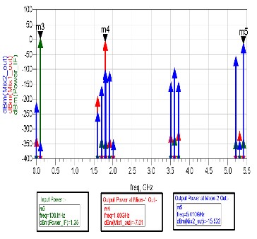
 Figure 12 : Output spectrum for the second iteration
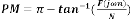
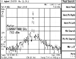
Figure 11 : RF Spectrum for the First iteration
The two iterations has been designed and simulated in ADS and there results are shown below. For the first iteration the local oscillator frequency (LO-2) is taken as swept variable an on changing this frequency according to the channel spacing different output required channels are obtained. And for the second iteration the VCO divider (N) value is changed in order to change the output of the frequency synthesizer and thus referring to the various required output channels. Here figure 11 and
12 shows the output spectrum for the first and second
iteration respectively. In figure 13 output spectrum obtained in the second iteration is shown followed by the description of power level of the signal at the various critical stages of the up-converter chain.
Figure 13 : Power levels at critical stages for the second iteration
There are also shown the measurement result for the frequency synthesizer and the final output for the up- converter portion.
http://www.ijser.org
IJSER © 20 12
International Journal of Scientific & Engineering Research Volume 3, Issue 4, April -2012 6
ISSN 2229-5518
Figure 14: frequency synthesizer output
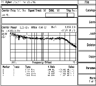
Figure 15: frequency synthesizer output phase noise
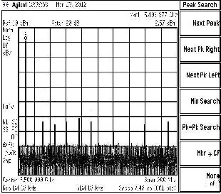
Figure 16: Up-converter measured final output for second iteration
5. CONCLUSIONS
 In figure 13, mixer 1 is giving output at -7.61 dBm with the input at +1.35 dBm thus for the calculation of mixer conversion loss is 8.16 dB.
 In figure 13, mixer 2 is giving output at -15.53 dBm with the input to the mixer 2 is at -7.61 dBm thus for the calculation of mixer conversion loss is 7.9 dB.
Thus, if we take a look at the output spectrum of both the iterations we can see that the output level in the second iteration is improved to the required level and the spurious level is further decreased by 5 to 6 dB. Thus, the signal separation from the spurious level is improved by
10 to 15 dB.
6. REFERENCES
[1] “An ultra broadband up converter circuit Auden tangs”, Stefan Johansson and Johan Lingsten Eriksson microwave systems, Se-431 84 Sweden.
[2] “C-Band Up and Down Converter Design Report”
EEE 787: MMIC design by Ray Gabany, Johns
Hopkins University 2000.
[3] “A Low Distortion C-band Double Balanced Up-
converter MMIC” C.H. Lee, S. Chakraborty, and I. Lascar School of ECE, Georgia Institute of Technology Yamacraw Design Center, Atlanta, GA
30332, USA ,2001.
[4] “A downsized and integrated C-band transceiver for
VSAT” Ge Zhiqiang; Microwave and Optoelectronics Conference, 1995. Proceedings, 1995 SBMO/IEEE MTT-S International Volume: 1 Publication Year:
1995 , Page(s): 33 - 36 vol.1
[5] “The up-converter with digital control for satellite
communication stations” Alybin, V.G.; Zyablikov,
S.Y.; Parusov, A.A.; E.Y.; Microwave Conference,
1999. Microwave & Telecommunication Technology.
1999 9th International Crimean Digital Object Identifier: 10.1109/CRMICO.1999.815141 Publication Year: 1999, Page(s): 55 – 56 Cited by: 1
[6] “Simulation of mathematical phase noise model for a
phase-locked-loop” 2000 Rangsi Watakapong and
Duangrat Eungdamrong Sirindhron International
Institute of Technology, Thammasat University.
[7] “ Fourth-order PLL loop filter design technique with invariant natural frequency and phase margin” by Thompson and P.V. Brennan; IEEE Proc.-Circuits Devices Syst., Vol. 152, No. 2, April 2005
[8] “Design and simulation of Fractional-N PLL
frequency synthesizers” By Mücahit Kozak and Eby
G. Friedman Department of Electrical and Computer
http://www.ijser.org
IJSER © 20 12
InternationalJournal of Scientific & Engineering Research Volume 3, Issue 4,April-2012 7
ISSN 2229-5518
Engineering University of Rochester
[9] PLL design by Dean Banerjee, PLL Techniques by Floyd M Gardener, Pozar, D. Microwave Engineering, Second Edition. John Wiley & Sons,
1998.
htto/Mr\NlN.ijser_ orq
IJSER <S>2012