The research paper published by IJSER journal is about Design and Analysis of CMOS Frequency to Voltage Converter using 0.35µm technology 1
ISSN 2229-5518
Design and Analysis of CMOS Frequency to
Voltage Converter using 0.35µm technology
Kopal Gupta, Monika Bhardwaj, Prof. B. P .Singh
Abstract—This paper presents a 0.35µm CMOS frequency to voltage converter for portable applications which is based on a operating principle comprises a differentiator, voltage to current converter, two RMS-DC converters, and a divider. Results show that the converter has a power consumption of 11.89mW operating at 3.3V supply voltage. This converter can accurately convert a sinusoidal signal frequency into an output voltage with no ripples . Moreover, its output response has input amplitude independent characteristic. The simulation results are in good accordance with the theoretical analyses.
Index Terms— Current mode Circuits, Differentiator, Divider, Frequency-to-Voltage Converter, RMS-DC Converter, Translinear principle, Tanner EDA ,Voltage to Current Converter.
—————————— ————— —————
requency to voltage or current converter is a device that generates an output voltage or current proportional to the frequency of a sinusoidal input signal. It has many applications in power control, communication, instrumentation and measurement systems, etc. The most known techniques used for frequency to voltage or current conversion are generally based on low-pass filtering of fixed duration at a rate set by the input frequency or counting the number of narrow pulses over a fixed period time [1-7]. Even though these techniques are widely used, they are based on complex circuits. Moreover, some of those have to use one or more reference signals with a very much higher frequency than the input signal. They are proposed by taking advantage of the mathematical characteristic of sinusoidal signals [8-9]. The frequency to voltage converter in [8] is realized by a differentiator, an integrator, a divider and a square-rooter. However, the division of the differentiator output to the integrator output causes large spikes when an initial value of the integrator is not zero. Unfortunately, an initial value of the integrator affects the converted output. Thus uncertain integral initial value makes the output of this technique inaccurate. In this paper, the frequency to voltage converter is presented which employs no additional integrators
comparing to the previous converter.
So the integral initial value which influences
the converted output as in [9] will not occur in the
proposed converter. In other words, this technique provides much better accuracy than the previous technique. The simulations are conducted to
confirm this idea and to illustrate the performances of the frequency to voltage converter. This paper is organized in six sections. Section 2 reviews the basic principle, circuit description and the implementation of Frequency to Voltage Converter. Simulation and Analysis of frequency to voltage converter is presented in Section 3 and finally the conclusions are reported in Section 4.
A frequency to voltage converter (FVC) is presented. It is composed of a differentiator, two RMS-DC converters, a divider and voltage to current converter. The block diagram is shown in Fig.1. Assuming that the input signal is a pure sinusoidal signal with a peak amplitude of A and input frequency of ωin,
![]() (1) Then, the derivative of this signal at the output of
(1) Then, the derivative of this signal at the output of
the differentiator can be written as
![]() (2)
(2)
where τd is the time constant of the differentiator. Feeding ![]() and
and ![]() into the voltage to current
into the voltage to current
converter and then to RMS-DC converters yields
the results as![]()
(3)
IJSER © 2012
The research paper published by IJSER journal is about Design and Analysis of CMOS Frequency to Voltage Converter using 0.35µm technology 2
ISSN 2229-5518
![]()
respectively.![]()
Thus dividing IRMS2 in (4) by IRMS1 in (3) yields
(4)
(5)
opposition. Capacitors oppose voltage change by creating current in the circuit: that is, they either
charge or discharge in response to a change in applied voltage. So, the more capacitance a capacitor has, the greater its charge or discharge current will be for any given rate of voltage change across it.
Figure3 shows the two stage op-amp based
where k is the sensitivity of the converter. It is
clearly seen from (5) that the output signal is
linearly proportional to the input frequency, ωin, and insensitive to the input signal amplitude, A.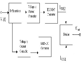
Fig. 1 Basic principle of the frequency to voltage converter
The differentiator is sometimes called the rate of change circuit. In differentiator, the capacitor is in series with the signal line while the resistor is in parallel with the line. In this, the RC time constant is short compared with the period of the signal [10]. The operational amplifier makes it relatively easy to build high quality active differentiator circuits. Previously, one had to construct a stable, drift free, high gain transistor amplifier for this purpose. Again, the RC elements are used, but in a slightly different manner. The capacitor is in series with the op-amp inverting input, while the resistor is in the op-amp feedback resistor.
By introducing electrical reactance into the
feedback loops of op-amp amplifier circuits, we
can cause the output to respond to changes in the input voltage over time. Differentiator produces a voltage output proportional to the input voltage's rate of change. Capacitance can be defined as the measure of a capacitor's opposition to changes in voltage.The greater the capacitance, the more the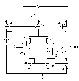
differentiator which measures change in voltage by measuring current through a capacitor, and outputs a voltage proportional to that current.
Fig. 2 Circuit diagram of differentiator
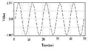
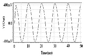
If the sinewave is applied to the input of differentiator then the result is the sinewave output that is shifted in –phase 90°.The circuit was simulated using T-Spice with 0.35μm TSMC CMOS process parameters. Vdd=3.3V, C1=60nF and R1=1k were employed. Fig. 3 (a) shows the time response of the differentiator for a sinusoidal input voltage with 1V peak amplitude and 100Hz frequency. Output of differentiator is cosine wave having peak amplitude of 400mV in Fig.3 (b).
IJSER © 2012
The research paper published by IJSER journal is about Design and Analysis of CMOS Frequency to Voltage Converter using 0.35µm technology 3
![]()
ISSN 2229-5518
3.3 1.904340e-004
The variation of supply voltage of frequency to voltage converter is represented graphically in Fig.
4.
(a) Input Voltage 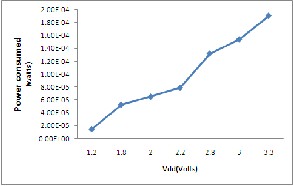
Fig. 4 Supply Voltage vs. Power Consumed Plot
(b) Output Voltage
Fig. 3 Time response of differentiator
The supply voltage is varied from 1.2 to 3.3V and then power consumed at different values of supply voltage can be obtained. Table1 shows values of power consumed for different values of supply voltages.
TABLE1
Power consumption with different supply voltage(VDD)
MOS translinear circuits can be categorized as follows [11]: stacked loop, up-down loop and electronically simulated loop. The stacked loop [12] similar to class-AB transconductance [13] suffers from body effect. Influence of the body effect in updown loop is smaller than in stacked loop but more circuits for current injection in transistors are required [14]. In Conventional circuit, a floating node in a circuit represents an error due to the fact that the initial condition is unknown unless it is somehow fixed. This generates two problems: first, it is not straight forward to simulate these circuits; and second, an unknown amount of charge might stay trapped at the floating gate during the fabrication process which will result in an unknown initial condition for the FG voltage as well as high power consumption and high cost. An RMS-to-DC Converter using electronically simulated translinear loop employing MOSFETs that are operating in saturation region is shown in Fig. 5. The circuit consists of three MOS transistors (M1, M2, and M3) and two op-amps. These two op-amps are employed for voltage mean operation and they force the gate voltage of transistor M3 to remain the mean voltage of the gate voltage of
IJSER © 2012
The research paper published by IJSER journal is about Design and Analysis of CMOS Frequency to Voltage Converter using 0.35µm technology 4
ISSN 2229-5518
![]()
transistors M1and M2. In other word, it can be written in mathematical form as follows:![]()
(6)
where Vg1, Vg2 and Vg3 are gate voltage of transistors M1, M2 and M3, respectively.
Fig. 5 Circuit diagram of the true rms-dc converter
Fig. 5 shows the circuit realization of the voltage mean operation, using transistors M4-M7 and current sources Ib1-Ib3.Employing the I-V relationships for transistors M1, M2 and M3 and the relations between current injections in translinear circuit and input/output currents of the squarer/divider are as the follows:![]()
![]()
By changing the sign of Iin [15] the equation remains unchanged. This means that the input of the squarer/divider is two-quadrant and acts as a full wave rectifier. From Fig. 5, the sources of translinear MOS transistors are connected to the substrate, so the body effect is completely eliminated.
For a current-mode first-order low-pass filter,
output current Ioutf and input current Iinf in Laplace domain are related as:
It can be shown that, for the input signal whose frequency is more than five times the cut-off frequency of the filter, output ripple will be less than 1% [16]. In such case, the output current of RMS-to-DC converter is a DC current Irms with an ac ripple on it. The amplitude of this ripple is small compared to Irms, i.e![]()
Considering these conditions it results that the values of the capacitor to achieve the accuracy of more than 1% is:![]()
![]()
is the lower end of the frequency range and is the output current higher end of the converter. The complete circuit diagram of the RMS-DC converter is depicted in Fig. 5. The circuit was simulated using T-Spice with 0.35μm TSMC CMOS process parameters. Vdd=3.3V, C=0.01pF and
Ib1=Ib2=Ib3=1uA were employed. Fig. 6 shows the
time response of the converter for a sinusoidal input current with 20μA peak-to-peak amplitude and 10 kHz frequency. The output is the dc current of 7.6µA which is same as rms value is shown in Fig. 6(b).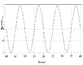
(a). Sinusoidal input current
IJSER © 2012
The research paper published by IJSER journal is about Design and Analysis of CMOS Frequency to Voltage Converter using 0.35µm technology 5
ISSN 2229-5518
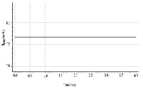
(b). Output Current
Fig. 6 Time response of the rms-dc converter
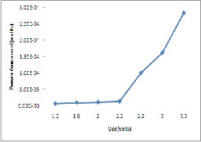
The supply voltage is varied from 1.2 to 3.3V and then power consumed at different values of supply voltages can be obtained. Table2 shows values of power consumed for different values of supply voltages.
TABLE2
Power consumption with different supply
voltage(VDD)
VDD (volts) | Power consumption (in watts) |
1.2 | 6.18E-06 |
1.8 | 9.28E-06 |
2.0 | 1.05E-05 |
2.2 | 1.30E-05 |
2.8 | 1.00E-04 |
3.0 | 1.62E-04 |
3.3 | 2.83E-04 |
The variation of supply voltage of frequency to voltage converter is represented graphically in Fig.7
Fig. 7 Supply Voltage vs. Power Consumed Plot
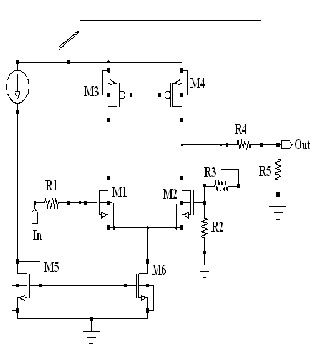
Fig. 8 Schematic of voltage to current converter
The circuit was simulated using T-Spice with
0.35μm TSMC CMOS process parameters.
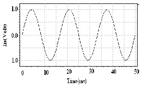
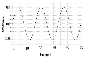
Vdd=3.3V, R1=R4=3.1ohm and R2=R3=R5=1ohm were employed.Fig.9 (a) shows the time response of the voltage to current converter for a sinusoidal input voltage with 1V peak amplitude and 100Hz frequency. Output of voltage to current converter is having peak amplitude of 200mA in Fig. 9 (b).
IJSER © 2012
The research paper published by IJSER journal is about Design and Analysis of CMOS Frequency to Voltage Converter using 0.35µm technology 6
ISSN 2229-5518
(a). Sinusoidal input voltage 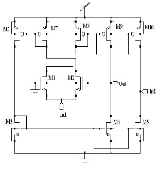
Fig. 10 Schematic of divider
(b). Output Current
Fig.9 Time response of voltage to current converter
Analog dividers do mathematical operation of division of two signals (voltage or current). The idea is shown in Fig.10, where all transistors are working in current saturation mode. In this MOS resistor M3- M4, M6-M7 and M8-M9 form current mirror pairs. M5 and M10 are output stage transistors of MOS resistor. The output resistance seen through the terminal B into the grounded resistor (Input A grounded) is equal to Rout. Input current In2 is applied and output voltage gives divider function given by
vout=In2*R![]()
Since the controlling current In1 has to be positive, this divider works only first-quadrant.
The circuit was simulated using T-Spice with
0.35μm TSMC CMOS process parameters Vdd=3.3V
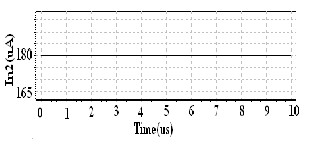
were employed. Fig. 11(a) shows the input current
In1 having dc value 90µA and In2 having
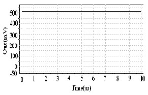
180µA.Fig. 11(b) shows the output voltage of
500mV.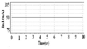
(a). Input Current In1 and In2
IJSER © 2012
The research paper published by IJSER journal is about Design and Analysis of CMOS Frequency to Voltage Converter using 0.35µm technology 7
ISSN 2229-5518
(b). Output Voltage
Fig. 11 Time response of the divider
All the circuits have been simulated using 0.35µm technology on Tanner EDA tool.
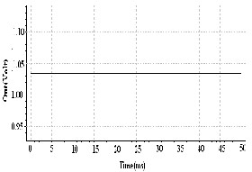
The complete circuit diagram of the frequency to voltage converter is depicted above in Fig.1. The circuit was simulated using T-Spice with 0.35μm TSMC CMOS process parameters with Vdd=3.3V. Fig.12 (a) shows a 1000 Hz sine wave signal with amplitude of 1 V which is applied at the input of frequency to voltage converter. Fig. 12(b) shows the dc output voltage of 1.04V without ripples.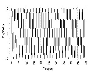
(a). Input voltage
(b). Output voltage
Fig.12 Time response of the frequency to voltage converter
To demonstrate the input-amplitude independent characteristic, the sinusoidal signals at 1000 Hz with varying amplitude from 1 V to 5 V are applied to the FVC. It yields the result as shown in Fig. 13. It is obvious that the characteristic is significantly flat as expected.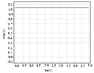
Fig. 13 Amplitude independent characteristics of frequency to voltage converter
The supply voltage is varied from 1.2 to 3.3V and then power consumed at different values of supply voltages can be obtained. Table3 shows values of power consumed for different values of supply voltages.
IJSER © 2012
The research paper published by IJSER journal is about Design and Analysis of CMOS Frequency to Voltage Converter using 0.35µm technology 8
ISSN 2229-5518
TABLE3
Power consumption with different supply voltage(VDD)
VDD (volts) | Power consumption (in watts) |
1.2 | 4.410055e-004 |
1.8 | 2.100061e-003 |
2.0 | 2.967266e-003 |
2.2 | 3.968086e-003 |
2.8 | 7.766710e-003 |
3.0 | 9.312802e-003 |
3.3 | 1.189842e-002 |
The variation of supply voltage of frequency to voltage converter is represented graphically in Fig.
14.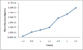
Fig.14 Supply Voltage vs. Power Consumed Plot
4 CONCLUSION
This paper has presented a technique of frequency to voltage converter. It is composed of a differentiator, voltage to current converter, two RMS-DC converters, and a divider. Since no additional integrators are exploited, it is superior to the conventional FVC because of no initial value effect. This FVC provides accurate measurements. The simulation results are in significant agreement with the theoretical. Moreover, the detected characteristic is independent of input amplitude.
The authors would like to thank Mody Institute of Technology & Science for supporting in carrying out this work.
[1] A.S. Hou, “Design of fast frequency-to-voltage converter using successive-approximation technique,” Int. J. Electron.,vol. 92, pp. 635-644, Nov. 2005
[2] M.K. Mahmood and J.E. Allos, “Fast frequency detection of sinusoidal signals,” Int. J. Electronics., vol.
54, No. 6, pp. 825-832, 1983.
[3] M.K. Mahmood, J.E. Allos, and M.A.H. Abdul- karim,“Microprocessor implementation of a fast and simultaneous amplitude and frequency detector for sinusoidal signals,” IEEE Trans. Instrum. Meas., vol.34, no.3, pp. 413-417, 1985.
[4] H.T. Bui and Y. Savaria, “High-speed differential frequency to voltage converter,” in Proc. IEEE North East Workshop Circuits Syst., 2005, pp.373-376.
[5] A. Djemouai, M.A. Sawan, and M. Slamani, “New
frequency-locked loop based on CMOS frequency-to- voltage converter: Design and implementation,” IEEE Trans. Circuits Syst. II Analog Digit. Signal Process,vol
48, pp. 441-449, 2001.
[6] W. Kiranon, P. Wardkein, and C. Loescharataramdee, “Simple frequency/voltage convertor with low output ripple,” Electron. Lett., vol.27, pp. 205-206, 1991.
[7] H.T. Bui and Y. Savaria, “Design of a high-speed
differential frequency-to-voltage converter and its application in a 5-GHz frequency-locked loop,” IEEE Trans. Circuits and Syst. I, vol. 55, pp. 766-774, 2008.
[8] W. Surakampontorn, Y. Chonbodeechalermroong, and S. Bunjongjit, “An analog sinusoidal frequency-to- voltage converter,” IEEE Trans.Instrum. Meas., vol. 40, pp. 925-929, Dec. 1991.
[9] T.Y. Lin, E.M. Drakakis, and A.J. Payne, “Architecture
for frequency-tocurrent conversion,” Electron. Lett.
, vol. 37, pp. 1427-1428, Nov. 2001.
[10] A.S. Sedra and K.C Smith,Microelectronics Circuits
New York:Oxford University Press,1991.
[11] E. Seevinck and R. J. Wiegerink, “ Generalized translinear circuit principle, ” IEEE J. Solid -State Circuits, vol. 26, no. 8, pp. 1098-1102,Aug. 1991.
[12] Bin-Da Liu, Chuen-Yau Chen and Ju-Ying Tsao, “A
modular current mode classifier circuit for template matching application,” IEEE.Trans. Circuits Syst.II, Analog Digit.Signal Processing, vol.47, no.2, pp.145-
151, Feb.2000.
[13] C. A. DE La Cruz-Blas, A. J. Lopez-Martin, A.
Carlosena and J. Ramirez-Angulo, “1.5v current-mode CMOS true RMS-DC converter based on class-AB transconductors, ” IEEE Trans. Circuits Syst. II,Express Briefs, vol. 52, no. 7, pp. 376-379, Jul. 2005.
[14] A. J. Lopez-Martin, and A. Carlosena, “A 1.5V current- mode CMOS RMS-to-DC converter, ”Analog Integrated Circuits Signal Process., vol.36, pp. 137-143, 2003.
IJSER © 2012
The research paper published by IJSER journal is about Design and Analysis of CMOS Frequency to Voltage Converter using 0.35µm technology 9
ISSN 2229-5518
[15] E. Farshidi, S. M. Sayedi, “A 1.2V current-mode true RMS–DC converter based on the floating gate MOS translinear principle,”Microelectronics Journal, Elsevier, vol. 39, no. 2, pp. 293–298, Feb.2008.
[16] D.R. Frey, Exact analysis of implicit RMS converters, Electron. Lett.40 (5) (2004) 1455–1456.

Kopal Gupta is currently pursuing her master’s degree in VLSI design at Mody Institute of Technology & Science, Laxmangarh. PH- 8058357751
Email: kopal2009@gmail.com

Monika Bhardwaj is currently working as faculty in ECE Department at Mody Institute of Technology & Science, Laxmangarh.
Email: monika19electrical @gmail.com

Prof. B. P. Singh is currently working as Head of ECE Department at Mody Institute of Technology & Science, Laxmangarh.
Email: bpsingh@ieee.org
IJSER © 2012