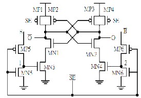
. Fig.1. Proposed Sense Amplifier[2]
International Journal of Scientific & Engineering Research, Volume 4, Issue 7, July-2013 402
ISSN 2229-5518
DESIGN OF HIGH SPEED AND LOW POWER SENSE AMPLIFIER FOR SRAM APPLICATIONS Shalini , Anand Kumar
Abstract: A high performance sense amplifier (SA) circuit for low power SRAM applications is presented in this work. My focus will be to improve the power consumption and response time of this sense amplifier. The transistor stage number of the proposed SA from V DD to GND is reduced for fast low voltage operation. Thus the proposed sense amplifier which is implemented in 0.18um CMOS process can work at 100MHz with voltage as low as 1.5V.Power consumption and delay have trade off,so we have to optimized the parameters according to our requirement.A great investigation is done in this thesis for power consumption and delay time. I observed the variation in these two parameters by varying the operating frequency,load and sizing of tail transistor of sense amplifier.
One of the major issues in the design of SRAMs is the memory access time (or speed of read operation). For having high performance SRAMs, it is essential to take care of the read speed both in the cell-level design and in the design of a clever sense amplifier. Sense amplifiers are one of the most critical circuits in the organization of CMOS memories. Their performance strongly influences both memory access time and overall memory power consumption. High density memories commonly come with increased bit line parasitic capacitances. These large capacitances slow down voltage sensing and makes bit line voltage swings energy-consuming, which result in slower more power hungry memories. Need for larger memory capacity, higher speed, and lower power dissipation imposes following trade offs in the design of sense amplifier:
1) Increase in number of cells per bit line increases the bit line parasitic capacitance.
2) Increasing cell area to integrate more memory on a single chip reduces the current that is driving the heavily loaded bit line. This causes smaller voltage swing on the bit line.
3) Decreased supply voltage lead to smaller noise
margin that affects the sense amplifier reliability.[1]
The proposed SA is shown in Fig. 1. We can observe that there are only three transistor stages cascaded from VDD to GND. Note that the transistor stage number is less than that of CLSA, and the input nodes B, Bbar are isolated to output nodes O, Obar.It is expected that the proposed SA has the same power consumption as CLSA, meanwhile a better performance at lower working voltage can be obtained.The circuit operation is described as follows.
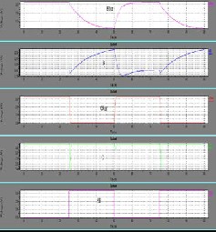
this mode, the data on output nodes must be cleared and the SA prepares for next sensing operation. Because the sensing signals SE=0 and SEbar =1, MP1, MP4, MN5 and MN6 turn on, meanwhile MP5, MP6 turn off.Thus the input signals from bit lines can’t enter through MP5 and MP6. Nodes 1 and 2 are pulled down to GND level by MN5, MN6, so MN3, MN4 will be cut off. The precharge transistors MP1, MP4 charge the output nodes to VDD. Because MN3, MN4 are turned off, both the output nodes will hold at VDD level. In this time interval, the operation detail is shown in Fig.2 (a).[2]
————————————————
. Fig.1. Proposed Sense Amplifier[2]
IJSER © 2013 http://www.ijser.org
International Journal of Scientific & Engineering Research, Volume 4, Issue 7, July-2013 403
ISSN 2229-5518
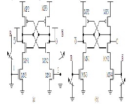
Fig.2. The proposed SA operation diagrams
(a)Precharge Mode (SE=0),(b) Sense Mode
(SE=1)[2]
We have completed the designing of the intended work. Our work consists of one memory cell, precharge circuitry connected with the bit lines pairs of memory. Our focus is to improve the power consumption and delay time of memory cell. Circuit diagram is shown in figure 3, which has been designed in Tanner S-edit and some parameters has been observed. Write circuitry consists of one memory cell, precharge circuitry connected with the bit lines pairs of memory shown in figure 4. For an analog designer, W/L ratio of a transistor is the main factor to achieve the desired objectives. We simulated the design for power consumption of the cell during read operation. We simulated the design and observed the power consumption which is shown in next chapter. By optimizing the value of W/L ratio of SRAM cell transistor, power consumption is improved.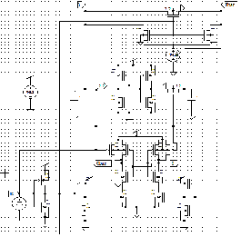
Fig.3. Designed Circuit Diagram in Tanner S-Edit Tool
We used Tanner tools- Schematic Editor (S-Edit), T-Spice and Waveform Editor (W-Edit) for simulating our design.
describing the simulation results for read ‘1’ operation. Designed block in S-Edit is simulated and simulated waveform is described here.
output voltage of Sense Amplifier. It is to read 1 from memory cell. Output voltage shows the logical 1 i.e. Vdd .. It is 0.637 ns.Sense amplifier enable signal also shown in figure.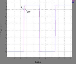
Fig.4.1. Output voltage of Sense Amplifer
4.2 shows the variation in bit line voltage. Bit lines first
IJSER © 2013 http://www.ijser.org
International Journal of Scientific & Engineering Research, Volume 4, Issue 7, July-2013 404
ISSN 2229-5518
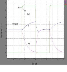
precharged to 1.65 V during prechage mode and when the memory cell is read, these voltage changes.
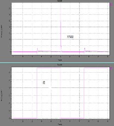
Fig.4.4 showing all signals in a single plot
Fig. 4.2. Showing variation in bitlines voltages

Fig.4.3: Showing variation in output nodes voltages
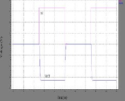
‘1’.Now I simulated the design for the cell which is storing
‘0’. I have explained the above simulation results and following results showing for memory cell when cell is storing ‘0’.
IJSER © 2013 http://www.ijser.org
International Journal of Scientific & Engineering Research, Volume 4, Issue 7, July-2013 405
ISSN 2229-5518
S.No. | Frequency (MHz) | Power consumption(mw) | Delay (ns) |
1 | 100 | 0.671 | 0.582 |
2 | 80 | 0.576 | 0.591 |
3 | 60 | 0.471 | 0.606 |
4 | 40 | 0.351 | 0.636 |
5 | 20 | 0.206 | 0.637 |
6 | 10 | 0.113 | 0.728 |
Fig. 4.6 Output voltage of sense amplifier during read 0
Table 4.2: Power Consumption and Delay at different load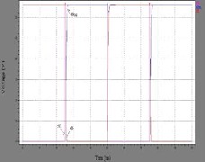
Table 4.3: Variation in Power Consumption and Delay with power supply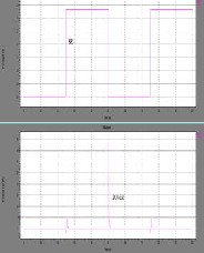
Table 4.1: Variation in Power Consumption and Delay
Table 4.4: Variation in Power Consumption and Delay with variation in transistor sizing
S.no. | Width of tail transistor of sense amplifier (um) | Power(mw) | Delay(ns) |
1 | 1 | 0.204 | 1.46 |
2 | 2 | 0.207 | 1.09 |
3 | 4 | 0.207 | 0.819 |
4 | 8 | 0.206 | 0.637 |
5 | 16 | 0.208 | 0.546 |
IJSER © 2013 http://www.ijser.org
International Journal of Scientific & Engineering Research, Volume 4, Issue 7, July-2013 406
ISSN 2229-5518
In this work, a low power high speed Sense Amplifier design for SRAM memory is presented. The power consumption and delay factors are improved by varying
the size of transistor used in Sense Amplifier..Sense amplifier is designed and simulated at 0.18µm technology. The design is implemented in CMOS technology. Power consumption and delay time of sense amplifier have been observed from simulation result. All results met specifications of the design.
[1].Kang, Sung-Mo and Leblebici, Yusuf, “CMOS Digital Integrated Circuits - Analysis and Design”, McGraw- Hill International Editions, Boston, 2nd Edition, 1999. [2].Hwang-Cherng Chow, Shu-Hsien Chang,“High Performance Sense Amplifier Circuit for Low Power SRAM Applications”,ISCAS IEEE 2004, 0-7803-8251.
[3].Adel S. Sedra and Kenneth C. Smith, “Microelectronics Circuits” Oxford University Press International Edition, New York, 5th Edition 2006.
[4].Ardalan,S.; Chen, D.; Sachdev, M.; Kennings, A.; “Current mode sense amplifier” Circuits and Systems, 2005.
48th Midwest Symposium Vol. 1, 7-10 Aug. 2005
Page(s):17 – 20.Tegze P.
[5].Haraszti, Microcirc Associates “CMOS Memory Circuits”,
kluwer academic publishers New York, boston , dordrecht, London, Moscow. Pages 238-239.
[6].Chun-Lung Hsu; Mean-Horn Ho; “High-speed sense amplifier for SRAM applications”,Volume 1, 6-9 Dec. 2004
Page(s):577 - 580 .
[7].Jan M. Rabaey, Anatha Chandrakasan and Borivoje Nikoliü, “Digital Integrated Circuits”, Pearson Education, Inc., Second Edition, p.p. 677, 2003.
[8].Kiyoo Itoh, “VLSI Memory Chip Design” Springer-Verlag
Berlin Heidelberg New York, p.p. 110, 2001.
IJSER © 2013 http://www.ijser.org