International Journal of Scientific & Engineering Research, Volume 4, Issue 6, June-2013 633
ISSN 2229-5518
Communicating Two FPGA’s using UART
Mercy Subaraman, Ravindra Asundi
Abstract— Presently FPGAs are coming very strongly in the digital hardware systems as it provides the opportunity for reconfiguration as well as good clock speed and design resources. The usage of FPGA systems in real time domain is also a very fruitful proposition as the FPGA devices are coming with processing cores for Real Time data processing. In a complex system scenario involving a large amount of processing tasks, there is a requirement of building the system using multiple FPGA devices. To make this possible we have to establish a real time data communication between the FPGA devices and to make it even better we have to apply data encryption techniques for making this communication secured.
Universal Asynchronous Receiver and Transmitter (UART) protocol is a kind of serial communication protocol; mostly used for short-distance, low speed, low-cost data exchange between computer and peripherals.. In particular, it focuses on their effective data transmission rates and ratios. UART includes three kernel modules which are the baud rate generator, receiver and transmitter. Furthermore, this paper describes the communication between multi- ple FPGA’s design using UART.
Index Terms— Communication, FPGA, UART
1 INTRODUCTION
—————————— ——————————
Reconfigurable System like FPGA platform has the poten- tial to provide the performance benefits of ASICs and the flexibility of processors. The recent development of Plat- form-FPGA or Field Programmable System-on-Chip ar- chitectures, with immersed coarse-grain processors, em- bedded memories and Implores, offers the potential for immense computing power as well as opportunities for rapid system prototyping. These platforms require high- performance on-chip communication architectures for ef- ficient and reliable inter-processor communication. How- ever, as the number of embedded processors increases, communication bandwidth between embedded compo- nents becomes a limiting factor to overall system perfor- mance. On-FPGA communication is important to provide high bandwidth and reliable data transfer between pro- cessing elements, and is therefore fundamental to overall FPGA-based system performance. In recently developed FPGA architectures, such as the so-called Platform-FPGA and Field- Programmable System-on-Chip, pre-fabricated coarse grained modules including microprocessors, DSP units and memory modules are immersed into the fine- grain programmable fabric. These can provide significant improvements in speed, area as well as hardware configu- ration time.
The Universal Asynchronous Receiver/Transmitter (UART) takes bytes of data and transmits the individual bits in a sequential fashion. At the destination, a second UART re-assembles the bits into complete bytes. Each UART contains a shift register, which is the fundamental method of conversion between serial and parallel forms. Serial transmission of digital information (bits) through a single wire or other medium is less costly than parallel transmission through multiple wires.Communication may be simplex (in one direction only, with no provision for the receiving device to send information back to the
IJSER © 2013
transmitting device), full duplex (both devices send and receive at the same time) or half duplex (devices take turns transmitting and receiving).

Fig 1: Character framing in UART
The idle, no data state is high-voltage, or powered. This is a historic legacy from telegraphy, in which the line is held high to show that the line and transmitter are not damaged. Each character is sent as a logic low start bit, a configurable number of data bits (usually 8, but legacy systems can use 5, 6, 7 or 9), an optional parity bit, and one or more logic high stop bits as shown in Fig 1.
The start bit signals the receiver that a new character is
coming. The next five to eight bits, depending on the code set employed, represent the character. Following the data bits may be a parity bit. The next one or two bits are always in the mark (logic high, i.e., '1') condition and called the stop bit(s). They signal the receiver that the character is completed. Since the start bit is logic low (0) and the stop bit is logic high (1) there are always at least two guaranteed signal changes between characters. If the line is held in the logic low condition for longer than a character time, this is a break condition that can be detected by the UART [3].
The sender does not know when the receiver has “looked” at the value of the bit. The sender only knows when the clock says to begin transmitting the next bit of the word. When the entire data word has been sent, the transmitter may add a Parity Bit that the transmitter generates. The
http://www.ijser.org
International Journal of Scientific & Engineering Research, Volume 4, Issue 6, June-2013 634
ISSN 2229-5518

Parity Bit may be used by the receiver to perform simple error checking (both the sender and receiver must agree on whether a Parity Bit may use or not) and when the receiver has received all of the bits in the data word then receiver looks for stop bit.
If the Stop Bit does not appear, the UART considers the entire word be garbled and will report Framing Error.
When the another word is ready for transmission, the start bit for the new word can be sent as soon as the stop bit for the previous word has been sent.
The UART takes bytes of data and transmits the
individual bits in a sequential fashion. At the destination,
a second UART re-assembles the bits into complete bytes. The UART allows the devices to communicate without the need to be synchronized. UART includes three kernel modules which are generator, receiver and transmitter. The paper focuses upon the effective communication between two FPGA’s using UART
2.UART DESIGN
UART provides the means to send information using a minimum number of wires. The data is sent bit serially, without a clock signal. The main function of a UART is the conversion of parallel-to-serial when transmitting and serial to- parallel when receiving. The fact that a clock signal is not sent with the data complicates the design of a UART. The two systems (transmitter and receiver) contain separate and unsynchronized local clocks. A part of the function of UART [5]
Communication between two FPGA’s using UART can be done effectively by sampling the incoming serial data at the right time to precisely capture the binary stream. This is ac- complished by utilizing a fast clock to sample the binary stream multiple times for each data bit. Thus, when transmit- ting, the UART receives the data in parallel from the applica- tion, and sends it serially on the TxD pin, and when receiving, the UART receives the data serially on the RxD pin, and pro- vides the parallel data to the application. The UART consists of two independent HDL modules. One module implements the transmitter, while the other module implements the re- ceiver. The transmitter and receiver modules can be combined at the top level of the design, for any combination of transmit- ter and receiver channels required. Data can be written to the transmitter and read out from the receiver, all through a single
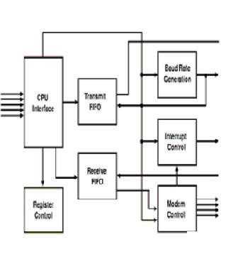
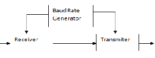
8 bit bidirectional CPU interface. Address mapping for the transmitter and receiver channels can easily built into the in- terface at the top level of the design. Both modules share a common master clock called mclkx16. Within each module, mclkx16 is divided down to independent baud rate clocks.The UART module is divided into three sub-modules: the trans- mitter module, receiver module and baud rate generator, shown in Fig. 3.
Figure 2: UART Block Diagram
2.1BAUD RATE GENERATOR
The Baud Rate Generator is used to produce a sampling signal which is much higher than the baud rate to control the UART receiver and transmit. The baud rate generator is actually a frequency divider. The frequency factor is calculated accord- ing
to the given system clock frequency and requested baud rate. Assume that the system clock is 4MHZ; baud rate is
9600bps.Therefore the frequency coefficient (M) of baud rate generator is:
M=4*10^6/9600Hz=416.666
Receiver clock (clk16) is 16 times faster than the internal clock
Clk16 = 416.666/16=26.
In order to obtain 50% duty cycle it needs to be further divid-
ed by 2.
Then clk16=13

Fig3
IJSER © 2013 http://www.ijser.org
International Journal of Scientific & Engineering Research, Volume 4, Issue 6, June-2013 635
ISSN 2229-5518

3. Proposed Design
2.2 RECEIVER
2.2.1 Receiver design
The receiver can be designed as a Finite State machine. The main goal of the receiver is to detect the start-bit, then de- serialize the following bit-stream, detect the stop-bit, and make the data available to the host. Three separate FSM’s should be the designed for start bit, data bits and stop bit. If the detected start bit is a real one, then it can sample the data every 16 times with respect to the clock 16x.
2.2.2 Clocking Issue
Our goal is to sample each bit at the midpoint .If we sample one-half a bit-period too early or too late, we will be sampling at the bit transition and have problems .In reality, we cannot sample close to the bit-transition point reliably. The primary reason for this is the finite (and typically slow) transmission rise and fall times. These times become even slower if overly capacitive cabling is used. A long bus incurs high attenuation, which reduces noise margin and makes it more important to sample when the bit level has settled.
2.3TRANSMITTER
The transmitter can be designed as a Finite State Machine as it increases the readability.Like the receiver counter-part, the design is minimalist and contains no error detecting logic. Transmission operation is simpler since it is under the control of the transmitting system. As soon as data is deposited in the shift register after completion of the previous character, the UART hardware generates a start bit, shifts the required num- ber of data bits out to the line, generates and appends the pari- ty bit (if used), and appends the stop bits. Since transmission
of a single character may take a long time relative to CPU
speeds, the UART will maintain a flag showing busy status so
that the host system does not deposit a new character for transmission until the previous one has been completed; this may also be done with an interrupt. Since full-duplex opera- tion requires characters to be sent and received at the same time, UARTs use two different shift registers for transmitted characters and received characters.
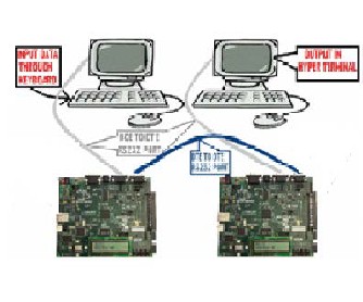
Fig.4. Proposed System using UART
This is the most challenging and interesting part of our paper, where two FPGA’s can communicate successfully. A real time data is taken from the Key board into board1 through RS232 port (DTE to DCE cable) and being sent to the board 2 through RS232 (DTE to DTE cable) port. The plain text is being send to the HyperTerminal of next PC through RS232 (DCE to DTE cable)
4. RESULTS

A real time data is received from the key board using the HyperTerminal application of a host computer which is then being sent to board using RS232(9600bps,no parity bits) serial cable in the DCE port on the board,receieving the data. The plain text is then transferred to the PC HyperTerminal via the RS232 DCE port (9600 bps, no parity bit.)
IJSER © 2013 http://www.ijser.org
International Journal of Scientific & Engineering Research, Volume 4, Issue 6, June-2013 636
ISSN 2229-5518

5. CONCLUSION
On-FPGA communication architectures play a crucial role in determining the performance and energy consumption
Of platform-FPGAs containing embedded coarse-grain mod- ules. The design of efficient and reliable communication archi- tecture is a challenging multi objectiveOptimization problem
.Here in this paper we have established reliable communica- tion between multiple FPGA’s using UART implementation with a reconfigurable baudrate generator. Future work can be done by incorporating an RTOS and implementing an inter- processes communication in the system
References
[1] Terrence S. T. Mak , Pete Sedcole, Peter Y. K. Cheung, On-
FPGA communication architectures and design factors.
[2] B.Jeevan & M.Neeraja, Design And Simulation Of Uart
Protocol Based On Verilog. Warangal.
[3] http://en.wikipedia.org/wiki/Universal_asynchronous_rec
eiver/transmitter.
[4] Gupta R.K., Zorian Y. (1997) IEEE Design & Test Of
Computers, 14-25.
[5] Magandeep kaur, ruchi mittal, FPGA implementation &
design of micro uart with different baud rates. Faridabad,
India.
[6]HazimKamalAnsari, Design of high Speed UART for program-
ming FPGA
IJSER © 2013 http://www.ijser.org
