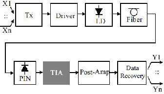
Fig. 1- The Optical Communication System
International Journal of Scientific & Engineering Research, Volume 3, Issue 10, October-2012 1
ISSN 2229-5518
Bandwidth Extension of Transimpedance Amplifier
Using Active Inductor
Keywords - active inductor, inductive peaking, optical receiver, shunt peaking, transimpedance amplifier, CMOS (Complementary metal oxide semiconductor), NMOS (n-channel metal-oxide-semiconductor)
—————————— ——————————
The performance of the optical interconnection system depends on the receiver’s gain, bandwidth, power consumption, and noise figure. These four parameters tend to trade-off with each other[3]. The front-end component of classic optical receiver generally is an amplifier. The low-noise characteristic is required by a typical amplifier in order to achieve a good noise performance of overall receiver system and the amplifier should operate as high of an input signal as possible without being saturated. The transimpedance amplifier has more noise due to feedback resistance but wide bandwidth and the proposed architecture is simple. In addition, the transimpedance amplifier has broad dynamic range due to the higher saturation limit. Thus, transimpedance amplifier (TIA) architecture is widely used in optical receiver systems.
Fig. 1- The Optical Communication System
Rohan Chadha is currently pursuing bachelor’s degree in Instrumentation and Control Engineering in Galgotias College of Engineering and Technology, Gr. Noida , India . E-mail id: rohanchadha41@gmail.com
Vibhor Mittal currently pursuing bachelor’s degree in Instrumentation and Control Engineering in Galgotias College of Engineering and Technology, Gr. Noida , India . E-mail id: vibs.mit6@gmail.com
Siddhant Mathur currently pursuing bachelor’s degree in Instrumentation and Control Engineering in Galgotias College of Engineering and Technology, Gr. Noida , India . E-mail id: sidd2308@gmail.com
Transimpedance amplifiers (TIA) are used in an optical receiver to convert small current signal (~10 μA) which are generated from the PIN diode to a voltage signal for post amplification and data recovery as shown in the figure 1. With the advancement in VLSI technology, CMOS circuits are widely used for high density applications because of low power consumption by these circuits. The design of multi- GHz range CMOS TIAs is explored in this paper for fulfilling the goal of “system on a chip” solution of the optical receivers. The primary factors that confine the signal bandwidth and noise performance of CMOS TIAs are the inherent parasitic capacitances introduced by the PIN diode and the bonding pad. A low input impedance TIA using regulated cascade and shunt feedback has been introduced in this paper. Inductive peaking technique using active inductor load is also used to enhance the gain and bandwidth of CMOS TIA. Active inductor is used as a substitute for the integrated spiral inductors because active inductors offer higher achievable on chip inductances and high quality factors while requiring a significantly smaller chip area than the conventional off-chip inductors. In addition, both the inductance and quality factor of active inductors can be tuned.
The circuit schematic of a typical low input impedance TIA is shown in figure 2 [2] which consists of a common gate input stage followed by a common source gain stage. The combination of CD-CS is widely used for broadband amplifier. The advantage of this configuration however lies in its bandwidth which is much wider than that obtained in a CS amplifier. The input capacitance is reduced by cascading of these two amplifiers and they provide low impedance at the gate node of CS [7].
IJSER © 2012 http://www.ijser.org
International Journal of Scientific & Engineering Research, Volume 3, Issue 10, October-2012 2
ISSN 2229-5518
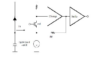
Fig. 2 - TIA with Low Input Impedance
The current distribution between CD and CS has the gain versus bandwidth tradeoff for a given total amount of current. If the more current are allocated to the CD stage than to the CS amplifier, less amount of resistance at the gate node of CS amplifier will be introduced while the voltage gain of CS is reduced because of lower current. At the gate node of CS amplifier, there exists Miller capacitance due to reduced gain. Therefore, more current allocation to CD stage results in wider bandwidth at the expense of gain. On the contrary, if more current is given to the CS amplifier, then the gate node of CS will have larger resistance as well as larger amount of parasitic capacitance because of higher gain of CS amplifier stage. Therefore, the overall gain of CD-CS will increase while the bandwidth decreases. More current are allocated to the CS stage of the CD- CS cascade in order to obtain higher amount of overall gain. To improve the bandwidth reduction by the higher amount of gain, inductive shunt-peaking technique has been applied using a novel active inductor load.
The resonance frequency determined by parallel-connected Lp1 and Ca should be near the desired corner frequency (f-3dB) in order to obtain bandwidth enhancement by the peaking phenomenon. The resonance frequency of Lp1 and Ca tends to be higher than 4GHz for a typical parasitic output capacitance Ca and for the reasonable value of on-chip inductor Ls (typically less than 15nH). However, the 3-dB bandwidth of the given amplifier is usually much less than that. Therefore, little improvement in bandwidth is provided by the conventional inductive shunt- peaking. In order to bring the resonance frequency close to the bandwidth, the inductance Ls has to be idealistically high.
To provide a large value of inductance to the shunt peaking amplifier architecture, novel active inductor architecture using NMOS has been proposed in this paper.
The circuit of CS amplifier with the proposed active inductor load is as shown in figure 4(a).[1] The small signal equivalent circuit
of the active inductor load is shown in figure 4(b) which is represented as Z out in figure 4(a). The output load impedance Z out can be derived as![]()
![]()
Where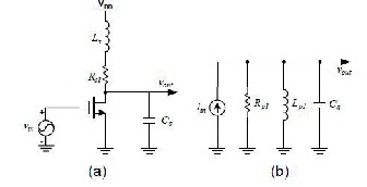
![]()
![]()
Where Q=![]()
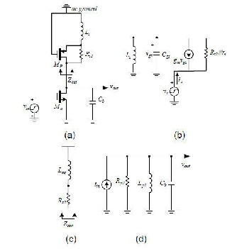
` (1a) (1b)
Fig.4
(a) A Shunt-Peaked Amplifier with Proposed Active Inductor load
(b) Small-Signal Equivalent Circuit for the Active Inductor
(c) Equivalent Circuit for fig. 5(b)
(d) Output Equivalent Circuit for fig. 5(a)
IJSER © 2012 http://www.ijser.org
International Journal of Scientific & Engineering Research, Volume 3, Issue 10, October-2012 3
ISSN 2229-5518
Zout represents a series connection of resistance Rs2 and an inductor with a multiplication factor as shown in equation (2). The inductive component of the output impedance approaches infinite as the frequency approaches the resonance frequency of Cgs·Ls. Therefore, at frequencies below the resonance frequency of Cgs·Ls, Zout becomes equivalent to Fig.4(c). Above the resonance frequency the second term of Eq. (2) becomes a capacitive. Thus, the shunt peaked amplifier of with the proposed novel active inductor load effectively becomes the same architecture like the typical shunt-peaked amplifier shown in Fig.
3(a). The difference is that the inductance Leq can be much larger than Ls, and the resistor Rs2 can also be larger value than Rs1. So, the output part of Fig. 5(a) can be represented as shown in Fig. 4(d). On comparing the schematic of Fig. 4(d) with Fig. 3(b), we obtain Lp2 is much larger than Lp1, and the capacitance Cb is slightly higher than Ca due to the additional capacitance from Mp. Therefore, the proposed active inductor load can induce inductive shunt peaking effect using practical inductor size at the desired frequency of 1 to 2 GHz range.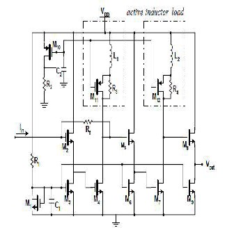
Figure 5 – Circuit diagram of TIA
As shown in figure 5, M2 and M3, M5 and M6 and M8 and M9 compose source follower circuit. M4 and M7 construct a common source amplifier with an active inductor load. M3, M6 and M9 are used as current sources of source-follower circuits. The cascade of M2 and M4, and the cascade of M5 and M7 are the Common- Drain (CD) and Common-Source (CS) combination (CD-CS). The combination of M8 and M9 are used as an output buffer. The Rf is the shunt feedback resistor and the C1 and C2 are used for ac ground. The rests are biasing circuit [2].
In this paper, the Broadband Amplifier has been proposed using
NMOS Active inductors. The circuit using NMOS active inductor
load has several advantages over the circuit using PMOS active inductor.
Figure 6 shows the TIA using PMOS active inductor load. The bandwidth obtained using this is 1.2GHz and a gain of 53dB has been obtained. The W/L ratio that was used in the original circuit for the PMOS active inductor was 1/.25u. The inductor was used in the circuit having value of 1nH.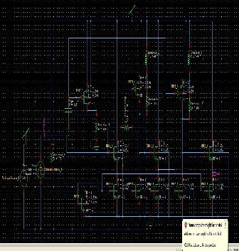
Fig.6- TIA Using PMOS Active Inductor Load
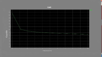
Fig.7- Simulation Result for Fig 6
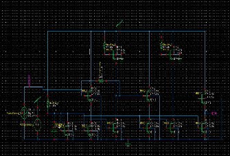
In the proposed work the PMOS active inductor is replaced by the NMOS active inductor. Along with that the W/L ratio has been increased to 1.25/.25u.
IJSER © 2012 http://www.ijser.org
International Journal of Scientific & Engineering Research, Volume 3, Issue 10, October-2012 4
ISSN 2229-5518
8. Gray Meyer, The Design of CMOS Radio Frequency Integrated Analysis and Design of Analog Integrated Circuits,3rd Edition, John Wiley & Sons, New York, 1997.
Figure 8- TIA Using NMOS Active Inductor Load
By the use of active inductor which is made up of parts such as load resistor, on-chip inductor, a PMOS transistor, the bandwidth of 2.2GHz is achieved. The active inductor which is proposed by us can be useful low frequency inductive peaking purpose. The TIA implemented on a 0.35 micron CMOS technology.
1. Yong-Hun Oh, Sang-Gug Lee, H.H.Park , “A 2.5 Gb/s CMOS Transimpedance amplifier using novel active inductor.”Solid state circuits conference, 2001, ESSCIRC 2001.
2 .Chao- Hsin Lu and Wei-Zen Chen “Bandwidth enhancement techniques for transimpedance amplifier in CMOS technology.” Solid state circuits conference, 2001, ESSCIRC 2001.
3. M. Nakamura, N. Ishihara, Y. Akazawa, and H. Kimura, “An Instantaneous Response CMOS Optical Receiver IC with Wide Dynamic Range and Extremely High Sensitivity Using Feed- Forward Auto-Bias Adjustment,” IEEE J. Solid-State Circuits, September 1995.
4 . S.B Baker and C.Thoumazou, “Low Noise CMOS Common Gate Optical Preamplifier Using Active Feedback.”Electronics Letters 1998.
5. S. M. Park and C. Toumazou, “Gigahertz Low Noise CMOS Transimpedance Amplifier,” IEEE International Symposium on Circuits and Systems, 1997, pp. 209-212.
6. T. Yoon and B. Jalali, “1Gb/s Fibre Channel CMOS Transimpedance Amplifier,” Electronics Letters, 1998.
7. Thomas H. Lee, The Design of CMOS Radio Frequency
Integrated Circuit, Cambridge University Press, New York,1998.
IJSER © 2012 http://www.ijser.org