International Journal of Scientific & Engineering Research, Volume 4, Issue 6, June-2013 2771
ISSN 2229-5518
Analysis and Characterization of Different
Comparator Topologies in 90nm technology
Aalay Kapadia (09BEC025@nirmauni.ac.in)1
Prof. Vijay Savani (vijay.savani@nirmauni.ac.in)2
Abstract— Comparator is one of the most important analog circuits required in many analog integrated circuits. It is used for the comparison between two different or same electrical signals. The design of Comparator becomes an important issue when technology is scaled down. Due to the non-linear behavior of threshold voltage (VT) when technology is scaled down, performance of Comparator is affected. Many versions of comparator are proposed to achieve desirable output in sub- micron and deep sub-micron technologies. The selection of particular topology is dependent upon the requirements and application. The different Comparator circuits have been analyzed using pre-layout simulation results for 0.5 μm . The comparative analysis table shows the advantages and disadvantages of different topologies. Some circuits have been proposed to remove limitations of basic Comparator. The advanced Comparator are now used in integrated circuits because they are successful in removing many of the limitations. Still, further advancement in necessary as downscaling of technology is increasing. The selection of topology is dependent on the required performance. In this paper, we have shown the implementation of different topologies in 0.090 μm technology using the Mentor Graphics Tool. We have done the pre-layout simulation of two different topologies. We have performed DC, AC and transient analysis. We have also calculated output impedance. We have prepared a comparative analysis about them.
Index- Voltage Gain, Output Impedance, Output Voltage
Swing, Power Dissipation.
I. INTRODUCTION
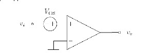
The schematic symbol and basic operation of a voltage comparator are shown in Fig. The comparator can be thought of as a decision-making circuit. If the +, v+' input of the comparator is at a greater potential than the -, v_ , input, the output of the comparator is a logic 1, whereas if the + input is at a potential less than the - input, the output of the comparator is at a logic O. Although the basic op-amp of the last chapter can be used as a voltage comparator, in some less demanding low-frequency or speed applications, we will not consider the op-amp as a comparator. Instead, we will discuss practical comparator design and analysis where propagation delay and sensitivity are important.

Fig 1. Basic Comparator Symbol
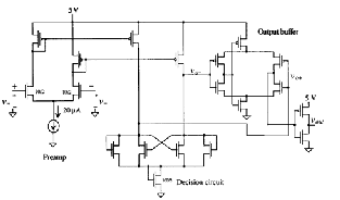
A block diagram of a high-performance comparator is shown in Fig.2. The comparator consists of three stages; the input preamplifier, a positive feedback or decision stage, and an output buffer. The preamp stage (or stages) amplifies the input signal to improve the comparator sensitivity (i.e., increases the minimum input signal with which the comparator can make a decision) and isolates the input of the comparator from switching noise coming from the positive feedback stage (this is important). The positive feedback stage is used to determine which of the input signals is larger. The output buffer amplifies this information and outputs a digital signal. Designing a comparator can begin with considering input common-mode range, power dissipation, propagation delay, and comparator gain.

II. BASIC COMPARATOR
The most basic version of the Comparator is the source follower. It is a common drain amplifier circuit with unity voltage gain. The output at the source terminal follows the input applied at the gate. The schematic of the circuit is shown in fig.1.
It is designed with the NMOS, PMOS and ideal current source. We can use current mirror also in place of current source. Comparator can also be designed with the resistor connected between source and supply. But it does not allow a constant current flowing through the source terminal. It results into non-linearity in the output and we can’t achieve unity voltage gain always. It also has high output impedance. So, resistive configuration is not used. We can use PMOS or
IJSER © 2013 http://www.ijser.org
International Journal of Scientific & Engineering Research, Volume 4, Issue 6, June-2013 2772
ISSN 2229-5518
NMOS as a load. But, the implementation with current mirror provides good results.

Fig 2.1. Basic comparator
The supply voltage requirement with is either 3.3V or 5V. In the basic source follower, the PMOSFET works in the

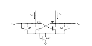
2.2 Decision Making stage:
Fig 2.3. Decision Making Circuit
The decision-making-circuit is the heart of the comparator and should be capable of differentiating between[3]mV level signals. We should be able to create a design of the circuit with some hysteresis for use in rejecting noise on a signal. The circuit used in the present comparator is shown in Fig 2.3[3]. The circuit uses positive feedback from the cross-gate
saturation region since
VDS - VGS
VTH .
connection of M6 and M7 to increase the gain of the decision
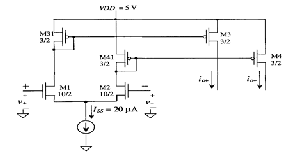
The most important parameter of Comparator is its output impedance. We can derive it from the small signal model shown in the fig.2.2 [ 6][9][10][18].
2.1 Pre-amplification Stage:

element[3]. Let's begin by assuming that io+ is much larger than io- so that M5 and M7 are on and M6 and M8 are off. We will also assume that ß5=ß8=ßA and ß6=ß8=ßB. Under these circumstances, vo_ is approximately 0 V and vo+ is
If we start to increase io- and decrease io+ switching takes place when the drain-source voltage of M7 is equal to VTHN of M6. At this point, M6 starts to take current away from M5. This decreases the drain-source voltage of M5 and thus starts to turn M7 off. If we assume that the maximum value of v0+ or v0- is equal to 2VTHN , then M6 and M7 operate, under steady-state conditions, in either cutoff or the triode regions. Under these circumstances, the voltage across M7 reaches VTHN , and thus M7 enters the saturation region, when the current through M7 is

i0 - =

(v0 + -vthn) =
2
B

i0 +
bA
Fig 2.2. Pre-amplification circuit
For Pre-amplification stage, it is important to concentrate on speed only so we are keeping length of channel to 2um for M1
This is the point at which switching takes place; that is, M7 shuts off and M6 turns on. If then switching takes place when the currents, io- and io+ are equal. Unequal ps cause the comparator to exhibit hysteresis. A similar analysis for increasing i: and decreasing t; yields a switching point of Relating these equations to Eq. yields the switching point voltages
Iss (bB - bA)
and M2.Using size shown in schematic we can relate input
voltage to output current, Here (W/L) of M1 and M2 is (10/2).

i0+= gm/2 (V+ - V-)+Iss/2 = Iss – i0- = 20uA - i0-. In this design case,
2(10)50 uA10uA
VSPH = v + -v- =
and
VSPL=-VSPH
gm (bB + bA)

;(bB - bA)
gm= gm1=gm2 = 2 v2
=71uA/V.
In other words, if V+ is greater than V- by 10mV then, i0+ And i0- will be 10.35 and 9.65 mA respectively. The desired output gain can be obtained by adjusting W/L ratios of two transistors M3 and M4.
2.3 Output Buffer:
The final component in our comparator design is the output buffer or post-amplifier. The only purpose of the output buffer is to convert the output of the decision circuit into a logic signal[3](i.e., 0 or 5 V). The output buffer should accept a
International Journal of Scientific & Engineering Research, Volume 4, Issue 6, June-2013 2773
ISSN 2229-5518

differential input signal and not have slew-rate limitations.
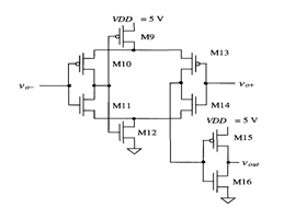
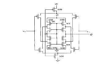
Fig 2.4. Output Buffer Circuit
The circuit used as an output buffer in our basic comparator design is shown in Fig. 2.4. This circuit is a self-biasing differential amplifier. An inverter is added in the output of the amplifier stage as an additional gain stage and to isolate load capacitance from the self-biased differential amplifier. The input vo+ is swept from 1 to 4 V, while va- is held at 1 to 3.5
V in 0.5 V increments. It is apparent that the inputs, vo+ and ,

vo- should lie within 1.5 and 3 V for linear operation of the output buffer. Comparing this result with the output of the positive feedback circuit, which varies from 0 to 1.5 V, we see a problem in connecting the decision circuit directly to the output buffer. For shifting the output of the decision circuit up approximately 1V, the circuit shown in Fig. 2.3 is used. The MOSFET M17 is added in series with the decision circuit to increase the average voltage out of the decision circuit. The size of the MOSFET is somewhat arbitrary. We will set W17/L17 =100um/2um.so that the output of the decision circuit is increased by approximately VTHN .The complete schematic of the comparator is shown in Fig.2.1. Unlabeled MOSFETs are 3 um/ 2 urn. Here, we scale down all the transistor size to use for 90nm technology.The table of scaled transistor is shown below:-
Table 1. PMOS dimension for Basic Comparator at 90nm
Transistor Name (W/L) MN1 0.9/0.18
MN2 0.9/0.18
MN3 0.9/0.18
MN4 0.9/0.18
MN5 0.9/0.18
MN6 0.9/0.18
MN7 90/0.18
MN8 0.9/0.18
MN9 0.9/0.18
MN10 0.9/0.18

Table 2. NMOS dimension for Basic Comparator at 90nm

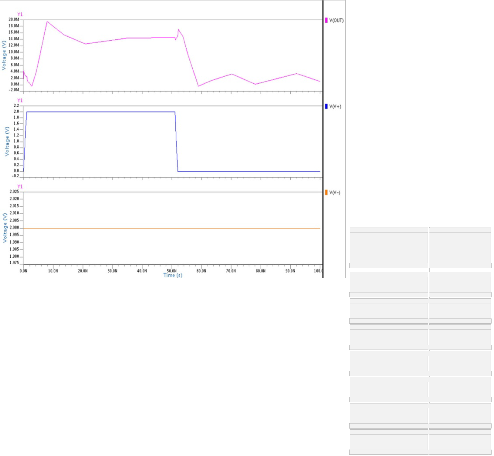
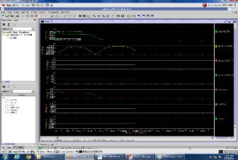
Fig 2.5. Transient Analysis of Basic Comparator at 90nm
IJSER © 2013 http://www.ijser.org
International Journal of Scientific & Engineering Research, Volume 4, Issue 6, June-2013 2774
ISSN 2229-5518

Fig 2.7.Basic Comparator
III. SELF BIASED COMPARATOR
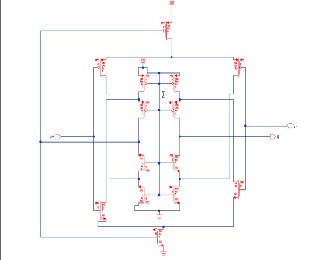
For the final example of a comparator, consider the self- biased comparator shown in Fig.3.1 [1]. This circuit operates similar to the self-biased differential amplifier but with a larger gain and wider input common-mode range. Note that because of the high gain of this comparator configuration, the delay tends to be longer (hundreds of ns) than the other configurations we discussed. The delay can be reduced, at the price of gain and more power dissipation, by decreasing the widths of Ml through M4 (operating Ml through M4 in the triode region) and by using minimum channel lengths.The scaled down Self-biased comparator’s transistor size is shown below.
Fig 2.6. Transient Analysis of Comparator at 90nm
The table based on simulation results of Comparator is shown in table-3.
Table 3
Simulation Results of Comparator
Table 6. PMOS dimension for Self-biased Comparator at 90nm

The implementation of Basic Comparator is shown in fig2.7
Transistor
Name
(W/L)

[1].
MN1 1.35/0.18
MN2 4.5/0.18
MN3 1.35/0.18
MN4 4.5/0.18
MN5 1.35/0.18
MN6 1.35/0.18
MN7 4.5/0.18
Table 5. NMOS dimension for Self-biased Comparator at 90nm
International Journal of Scientific & Engineering Research, Volume 4, Issue 6, June-2013 2775
ISSN 2229-5518


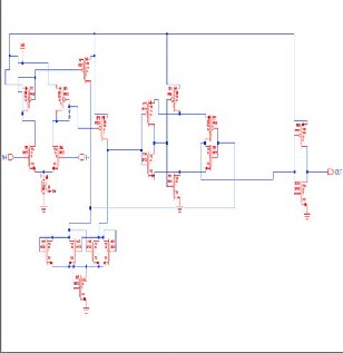
Fig 3.1. Self Biased Comparator 

Fig 3.4 Self Biased Comparator in 90nm technology

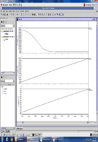
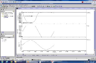
Fig 3.2Transient analysis of Self Biased Comparator
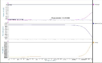
Fig 3.3 A.C. analysis of Self Biased Comparator
Fig3.5 A.C. Analysis of Self Biased Comparator
Table-4 shows the simulation results of Self-Biased
Comparator.
Table 4
Simulation Results of Self Biased Comparator
The number of transistor of Self Biased Comparator is decreased to 14, it decreases the size. So it limits the output swing in deep sub micron technology. This is the major disadvantage of Self Biased comparator topology.
IJSER © 2013 http://www.ijser.org
International Journal of Scientific & Engineering Research, Volume 4, Issue 6, June-2013 2776
ISSN 2229-5518
IV. COMPARATIVE ANALYSIS
Table 5
Comparative Analysis
Topology | Voltage Gain | Bandwidth | No. Of Transistors |
Basic Comparator | 3500 | 600MHz | 17 |
Self Biased Comparator | 7000 | 25.80 MHz | 14 |
The comparative analysis of all two topologies is shown in table-3. It explains the advantages and disadvantages of all three circuits. Output impedance is low and better in case of threshold independent Comparator and Self Biased Comparator. Bandwidth is higher in case of Basic Comparator has high power dissipation because of requirement of large biasing current. Both topologies provide approximately high voltage gain.
V. CONCLUSION
This paper explains about the Comparator and its design in sub-micron and deep sub-micron technologies. The two topologies of comparators have been implemented in 0.090 μm technology and brief comparison between them is made by analyzing pre-layout simulation results. The basic parameters need to be considered in any design is output impedance and voltage gain. Comparison table shows that different circuits have different advantages and disadvantages.. Threshold independent Comparator provides zero offset voltage. It is having many advantages compared to the other versions. Still, But, the selection of any topology is based on the application and the requirements. In 90 nm technology, due to small-scale effects found in MOS, Comparator behave non-linearly. This non-linearity decreases as we go for higher topology. So non- linearity effect should also be taken care for particular application.Simulations in 90 nm technology also show that operating bandwidth of current mirror increases far from 0.5
µm technology.Power dissipation also reduces in 90 nm due to small active area.
V. REFERENCES
[1] harry w. li, r. jacob baker and david e. boyce, cmos circuit design, layout and simulation, ieee press series on microelectronic systems, 2005.
[2] yahoui kong, shuzheng xu and huazong y, “an ultra low output resistance and wide swing voltage follower”, icccas 2007, pp. 1007-1010, july 2007.

[3] “high-efficiency low-voltage dc-dc conversion for portable applications", located on: http://people.sabanciuniv.edu/~yasar/dc-dc-converter.pdf

[4] "rayleigh distribution definition", located on: http://www.enfocus.com/content/en- us/documents/partnersitefile/pdf_standards.pdf http://bricxcc.sourceforge.net/nbc/nxcdoc/nxc_tutorial.pdf

[5] "tvcgsi-0011-1102 shadows and soft shadows with participating media using splatting", located on: http://www.cse.ohio- state.edu/~crawfis/publications/shadow_tvcg.pdf

[6] "monitoring and early warning for internet worms", located on: http://www.cs.utsa.edu/~shxu/cs6973-
fall2005/papers/zou-ccs03.pdf
[7] "a comparative study of supervised learning techniques for the radiative transfer equation inversion", located on: http://www.iaeng.org/publication/wcecs2007/wcecs2007_ pp683-688.pdf

[8] "multisensor data fusion implementation for a sensor based fertilizer application system", located on: http://ecommons.library.cornell.edu/bitstream/1813/10605
/1/atoe 07 010 ostermeier 11july2007.pdf

[9] "draft types as graphs: continuations in type logical grammar", located on:

http://semanticsarchive.net/archive/de2ytm1n/barker- shan-tlg.pdf

[10] "abstract exploring human judgement of digital imagery", located on: http://crpit.com/confpapers/crpitv62volkmer.pdf

[11] "design and implementation of fan motor driver ic with pwm speed control", located on: http://etd.lib.nsysu.edu.tw/etd-db/etd- search/getfile?urn=etd-0715105-025051&filename=etd-
0715105-025051.pdf

[12] "submitted 1 fixed-order robust h ∞ controller design with regional pole assignment", located on: http://homepages.laas.fr/henrion/papers/hinfpoly.pdf

[13] "the use of the deanza ip6400 image processor for local window operations", located on: http://deepblue.lib.umich.edu/bitstream/2027.42/4537/4/b ab3418.0001.001.txt http://deepblue.lib.umich.edu/bitstream/2027.42/4538/4/b ab3425.0001.001.txt

[14] dynamic response of a mobile offshore base advisory committee: hydroelastic test model by", located on: http://www.library.umaine.edu/theses/pdf/venkataramanv
2001.pdf

[15] "why do good people steal intellectual property?", located on: http://www.bepress.com/cgi/viewcontent.cgi?article=1017
&context=giwp

[16] "“High-Efficiency Low-Voltage DC-DC Conversion for Portable Applications", located on: http://people.sabanciuniv.edu/~yasar/dc-dc-converter.pdf

[17] "Abstract Exploring Human Judgement of Digital Imagery", located on: http://crpit.com/confpapers/CRPITV62Volkmer.pdf
International Journal of Scientific & Engineering Research, Vo lume 4, Issue 6, June-2013
ISSN 2229-5518
2777
[18] TVrGSl-()()11- 11m Shadnw. and Snft Shadnws with Partir:inatinf> Media Using Splatting" , located on: httn -1/www r.ohio-
state. eduf"-'Crawfi.s/Publications/shadow tvcg. pdf
I£ER 2013 http://WWW.IISer. org
