International Journal of Scientific & Engineering Research, Volume 5, Issue 12, December-2014
ISSN 2229-5518
1420
Analysis And Design Fastest Adder
Using Transmission Gate Logic
Prerana Shrivastava
Pru.rewa@gmail.com
Abstract:
The conventional carry look ahead adder (CLA) Require larger gate count as compare to the parallel adder, but it is a common viewpoint that area can be traded off in order to achieve speed. In our work the use of transmission gate reduces the number of transistors which overcomes the area trade of. The objective of our thesis is to design a high-speed adder, along with lower-power and smaller area as a prime consideration. A Complementary Metal Oxide Semiconductor (CMOS) Transmission Gate (TG)- based carry lookahead adder 4-bit block has been designed. This 4-bit block is designed to be connected to other 4-bit blocks to form higher bit adders.
Keywords: Ripple carry adder, CLA, TG, Carry Generator, Carry Propagator, FA.
Introduction:
Parallel adders also called as ripple carry adder are digital circuits that do the addition of two binary datas of equivalent or different size in concurrent. The parallel adder is design by cascaded connection of full adders (FA) blocks. Every full adder add two binary digits at any stage of the ripple carry. The carryout of one stage is connected directly to the carry input of the next stage. The carry propagation from one full adder to its cascaded stage reduces the speed of the parallel adder circuits its main drawback due to the time it takes to propagate the carry. To defeat this limitation we propose the carry look ahead adder (CLA) design by using transmission gates which solves this problem by calculating the carry signals in advance, based on the input signals. The conventional ripple carry adder have speed limitation due to the carry propagation.
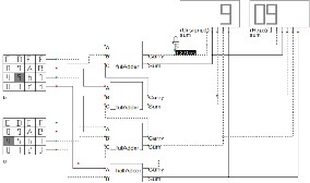
Fig 1 Schematic circuit for parallel adder logic.
The parallel adder is design by cascaded connection of full adders (FA) blocks. Every full adder adds two binary bits at any stage of the ripple carry. The output carry bit of one stage is connected to the carry input of the next stage full adder. Fig 1 shows an example of a parallel adder: a 4-bit ripple-carry adder with the input connected to 4X4 keyboard and output is connected to the seven segment display. Each one bit addition creates a sum and a carry output. The carry output is then pass to the carry in of
the next stage higher-order bit. At the last result creates a sum of four bits plus a carry out (Sc4).
IJSER © 2014 http://www.ijser.org
International Journal of Scientific & Engineering Research, Volume 5, Issue 12, December-2014
ISSN 2229-5518
1421
Transmission Gate :
Transmission gate can be operate like a switch with low resistance and capacitance and the DC characteristic of this gate are independent of the input levels. It is design by connecting both source to source and drain to drain terminals of NMOS and PMOS transistors respectively. As the NMOS transistor is passing strong ‘0’ signal i.e it discharge the output level to zero and PMOS transistors passes strong ‘1’ signal towards the output i.e it charge the output to logic high, the enable signal will turn on or off both transistor at a time. Sizing of transistor is varies as the resistance and capacitance decrease and increase respectively with the gate W/L ratio is increased. The worst-case delay of a cascade connected of pass transistors can be modelled by the linearized RC network. The on resistance of the transmission gate is determined, and is modelled out by a resistor and diffusion capacitance is also modelled for each transistor.
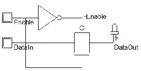
Fig 2 Transmission Gate Schematic.
The Fig 1 and fig 2 shows the transmission gate schematics and its layout design. If we applied input enable equal to logic ‘1’ then both P and N MOSFET turn on and data out follows the input Data in. Otherwise both the N and P MOSFET transistors are turn off and output remains latched. The fig 2 shows the RC delay model designed for transmission gate chain.
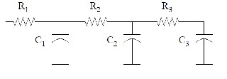
Fig 3 RC delay model for transmission gate chain. The propagation delay is calculates as:
Td = 0.69∑𝑁
𝐶�
�
�=1
𝑅�
Td = 0:69 (C1R1 + C2 (R1 + R2) + C3(R1 + R2 + R3) )
With the decrement of resisteance of first transmission gate in the series chain will increase the diffusion capacitance. Thus the increase in MOSFET channel length will not alter the delay at all. Increasing the MOSFET channel width ‘W’ of a transmission gate transistors will also increase the gate capacitance which will load the select signal, S, more heavily. Based on the logic above, we can conclude that to
design low power circuit, the size of transmission gates should be made as small as possible.
IJSER © 2014 http://www.ijser.org
International Journal of Scientific & Engineering Research, Volume 5, Issue 12, December-2014
ISSN 2229-5518
1422
Carry look-ahead adder:
As seen in the ripple-carry adder, its limiting factor is the time it takes to propagate the carry. The carry look-ahead adder solves this problem by calculating the carry signals in advance, based on the input signals. The result is a reduced carry propagation time. The basic building blocks in this adder is the PG generator, carry generator and sum generator.
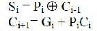
The working operation of carry look ahead adder can be understand by its Boolean equation very well. The exclusive or operation of two inputs is given as Pi = A xor B, and the carry generate operation is given by Gi = Ai.Bi. Thus both propagate and generate signals depend only on the input bits and thus will be valid after one gate delay.
The new expressions for the output sum and the carryout are given by:
Consider the addition of two four bit numbers a3a2a1a0 and b3b2b1b0 The unity carry at the ith stage can be expressed in term of Gi, Pi Ci-1 which is the unit carry output of 9i-1)th stage as:
Cout = Gi + Pi Ci-1
Where Ci-1 for i.e Cin is assume to be 0. In a four bit binary Adder , four stage of binary addition is required to add A0B0, A1B1, A2B2, and A3B3 thus the carry generator Boolean equation
is given as:
C0 = G0 + P0Cin
C1 = G1 + P1Co
= G1 + P1 (G0 + P0Cin) C2 = G2 + P2C1
= G2 + P2 (G1 + P1 (G0 + P0Cin)) C3 = G3 + P3C2
= G3 + P3 (G2 + P2 (G1 + P1 (G0 + P0Cin))
Propose Logic CLA:
The Boolean equation of carry lookahead logic of C0, C1, C2, C3 etc for carry generator requires large number of gates. This is the main drawback of carry look ahead adder as it require large number of transistor as compare to ripple carry parallel adder. So to reduce this gate count we propose the transmission gate base design which requires less number of transistors.
A transmission gate is an analog switch operate by logic signals. It consists of a NMOS and a PMOS transistor with source –source and drain- drain connected terminals. Transmission Gate is a switch with low resistance and capacitance. Sizing is also not necessary in general, as the resistance and capacitance decrease and increase respectively as the gate W=L ratio is increased. Fig 4 shows the schematic
diagram of carry generator design by transmission gate logic.
IJSER © 2014 http://www.ijser.org
International Journal of Scientific & Engineering Research, Volume 5, Issue 12, December-2014
ISSN 2229-5518
1423
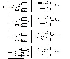
Fig 4 Propose carry generator for CLA using transmission gate.
The fig 5 shown is the 8 bit carry look ahead adder design by using transmission gate logic. The inputs (a0,b0 ), (a1,b1), (a2,b2), and (a3,b3), (a4,b4) (a5,b5) (a6,b6) (a7,b7) can be added which generates the sum output Pi and carry output Gi. These outputs are again connected to the carry generator logic circuit mention in fig 4. The 8 bit output sum0, sum1, sum2, sum3, sum4 sum5 sum6 sum7 Along with eighth carry out and sumc7 is taken form XOR logic circuit.
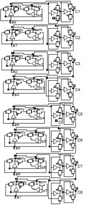
Fig 5 Propose Schematic design for 8 bit CLA Adder.
The PG generator is design by using the transmission gate base AND gate logic and XOR gate logic.PG generator is a combinational circuit that performs the arithmetic sum of two input bits. It consists of two inputs and two outputs P and G. Two of the input variables can be defined as Ai and Bi and the two
output variables can be defined as Pi for sum and Gi for carry.
IJSER © 2014 http://www.ijser.org
International Journal of Scientific & Engineering Research, Volume 5, Issue 12, December-2014
ISSN 2229-5518
1424
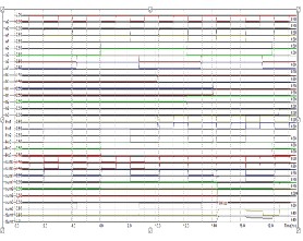
Fig Timing simulation for logic circuit for 8 bit CLA adder.
A transmission gate use in above design is an analog switch controlled by logic signals. It consists of a n and a p type MOS transistor. When the EN = 1 the gate conducts and shorts the input and the output, otherwise it cuts off and the output floats. We can design the basic building blocks of carry look ahead adder by using transmission gate. Transmission Gate has the ability of a high-quality switch with low resistance and capacitance. Sizing is also not necessary in general, as the resistance and capacitance decrease and increase respectively as the gate W=L ratio is increased. TG is commonly used to implement designs with the minimum number of transistors. Fig 5 shows the schematic diagram of carry generator design by transmission gate logic.
Table 1 Comparative analysis
Module design | In paper [1] | Our work |
4 bit | 0.215ns | 0.09ns |
8 bit | 0.352ns | 0.18ns |
16 bit | 0.616ns | 0.36ns. |
32 bit | 1.115ns | 0.72ns |
The proposed design circuit has been use for the implementation of 8-, 16-, 32-, and 64-bit adders using transmission gate base logic design, and the timing simulation of its layout results verified its efficiency.
Conclusion:
The use of pass transistor transmission gate logic is much more power-efficient than complementary CMOS. This work shows that for low power applications in 50nm technology, CLA adder implementation is superior to the other adder logic style because of its reduce number of transistors and low average power of 1.596 uW. The total number of transistors require to design our logic circuit is
128 which is less than 184 number of transistors required for four bit conventional CLA adder.
References:
[1] Mikhail Dorojevets, Christopher L. Ayala,Nobuyuki Yoshikawa, and Akira Fujimaki "16-Bit Wave- Pipelined Sparse-Tree RSFQ Adder" IEEE Transactions On Applied Superconductivity, Vol. 23, No.
3, June 2013 pp no. 17605.
IJSER © 2014 http://www.ijser.org
International Journal of Scientific & Engineering Research, Volume 5, Issue 12, December-2014
ISSN 2229-5518
1425
[2] Yu-Shun Wang, Min-Han Hsieh, James Chien-Mo Li, and Charlie Chung-Ping Chen "An At-Speed Test Technique for High-Speed High-order Adder by a 6.4-GHz 64-bit Domino Adder Example" IEEE Transactions On Circuits And Systems—I: Regular Papers, Vol. 59, No. 8, August 2012 pp no. 1644.
[3] Costas Efstathiou, Zaher Owda, and Yiorgos Tsiatouhas "New High-Speed Multi output Carry Look-Ahead Adders" IEEE Transactions On Circuits And Systems—Ii: Express Briefs, Vol. 60, No. 10, October 2013 pp no. 667
[4] Hafiz Md. Hasan Babu, Lafifa Jamal and Nazir Saleheen " An Efficient Approach for Designing a
Reversible Fault Tolerant n-Bit Carry Look-Ahead Adder" IEEE conferemce year 2013.
IJSER © 2014 http://www.ijser.org