
International Journal of Scientific & Engineering Research, Volume 4, Issue 7, July-2013 1708
ISSN 2229-5518
Yogesh N. Thakre, Shubhada S. Thakare, Devendra S. Chaudhari
Abstract— This paper deals with the design and analysis of 3T-1D DRAM cell to develop process variation architecture using Tanner EDA Tool. In this paper power dissipation analysis for DRAM design have been carried out for different nanotechnology with different voltages. The major contribution of power dissipation in DRAM is off –state leakage current. Thus improving the power efficiency of DRAM is critical to the overall system power dissipation. Generally process variation will greatly impact the stability, leakage power consumption and performance of future microprocessor. The absence of the capacitor is advantageous in terms of scalability, process and fabrication complexity, compatibility with the logic processing steps, device density, yield and cost. In this paper, 3T-1D DRAM cell are designed with schematic design technique of Tanner EDA Tool for the comparison of power dissipation.
Index Terms— Dynamic RAM (DRAM), Cell, Power Dissipation, 3T-1D (Three transistor- one diode), leakage, technology, etc.
—————————— ——————————
ECHNOLOGY nanoscaling promises increasing transistor density and increasing performance in microprocessor. In modern microprocessor on chip memory consume a sig- nificant portion of overall die space, providing high system performance in exchange for the space and power they con- sume. [1] As continuous technology change for high density memories favors small memory cell sizes, the dynamic RAM cell with a small structure has become a popular choice, where binary data are stored as a charge in a capacitor and the pres- ence or absence of stored charged determine the value of stored bit. The data stored in a capacitor based DRAM cell cannot retain indefinitely, because the leakage current eventu- ally remove or modify the stored data. Thus the capacitor based DRAM required periodic refreshing of the stored data, so that unwanted modification due to leakage is prevented before they occur. Also scaling of this capacitor is critical job; hence to avoid scaling limitation new circuit and architecture solution are needed. The problem of scaling and leakage – as well as device size – rests fundamentally with the basic tran- sistor/capacitor building block. While the transistor element is theoretically scalable – at least for the foreseeable future – the capacitor is not. Capacitors can be fabricated as high stacks above the wafer surface or deep trenches inside the wafer to maximize the surface area and thus the capacitance per unit footprint area. However, if the overall bit cell size shrinks due to increased density or a smaller process node, then the capac- itor will have to be made higher or deeper in order to maintain the minimum charge required for reliable operation. We are fast approaching the scaling limits for the capacitor ele- ment, and a new approach or a DRAM replacement will be
————————————————
• Yogesh N. Thakre, Department of Electronics and Telecommunication, Government College of Engineering, Amravati, India, +919975629591, (e- mail: yash4767@gmail.com).
• Shubhada S. Thakare, Department of Electronics and Telecommunica-
tion, Government College of Engineering, Amravati, In- dia,+919637277216, (e-mail: thakare.shubhada@gcoea.ac.in).
• Dr. Devendra S. Chaudhari, Department of Electronics and Telecommu- nication, Government College of Engineering, Amravati, India,
+919421821030, (e-mail: ddsscc@yahoo.com).
needed. In this paper, we design on chip memory architecture based on 3T-1D dynamic memory cell without capacitor.
2 COMPARISON BETWEEN 1T-1C AND 3T-1D DRAM
Dynamic random access memory (DRAM) is a type of random access memory. DRAM cell consists of one transistor and one capacitor. Capacitor stores the information in terms of the charge and the transistor is used to write and read the stored information. Each bit of data is stored in a separate capacitor within an integrated circuit. Due to the leakage of the capaci- tors, the information eventually fades unless the capacitor charge is refreshed periodically. This refresh requirement makes DRAM a dynamic memory as opposed to a static memory.
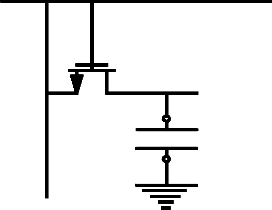
Dynamic random access memory (DRAM) is a type of memory that stores each bit of data in a separate capacitor within an integrated circuit. The basic DRAM cell consists of one transistor and one capacitor as shown in Fig.1. Due to the leakage of the capacitors, the information eventually fades unless the capacitor charge is refreshed periodically. This re- fresh requirement makes DRAM a dynamic memory as op- posed to SRAM (Static random access memory).
Recently the capacitorless single-transistor (1T) DRAMs have attracted attention, due to the lack of the capacitor and the problems associated with the scaling of the capacitor, and due to its ability to achieve higher device density. The infor- mation is stored as different charge levels at a capacitor in conventional 1T/1C DRAM. The advantage of DRAM is its structural simplicity: only one transistor and a capacitor are required per bit, compared to six transistors in SRAM. This allows DRAM to reach very high density.
IJSER © 2013 http://www.ijser.org
T1

International Journal of Scientific & Engineering Research, Volume 4, Issue 7, JBulyL-2013 1709
ISSN 2229-5518
WL
T1
BL
C STORE
C STORE
boosts up the turn-on voltage of T2, rapidly discharging the
bitline. As a result, the access speed can match the speed of 6T
SRAM cells. Conversely, when a “0” is stored, the capacitance
of D1 is smaller and there is almost no voltage boosting, which
keeps T2 off during the read. Hspice simulation results, shown
in Figure 2, illustrate the operation of the 3T1D cell. The gate
voltage of T2 is boosted by about 1.5-2.5 times (1.13V) the orig-
inally stored voltage (0.6V) if a “1” is stored when being read.
Although the speed of a 3T1D cell can be fast, this high-speed
access is only valid for a limited time period after each write to
the cell. This is because the charge on D1 leaks away over
time. With this stored charge leaking away, the access time
increases until finally it exceeds the array access time of the 6T SRAM cell. Traditionally, the word “retention time” is defined as the time a DRAM cell can no longer hold the stored value.
Fig.1: One transistor- one capacitor DRAM
The DRAM industry has achieved miracles packing more and more memory bits per unit area in a silicon die. But, the scaling of the conventional 1Transistor/1Capacitor (1T/1C) DRAM is becoming increasingly difficult, in particular due to the capacitor which has become harder to scale, as device ge- ometries shrink. Apart from the problems associated with the scaling of the capacitor, scaling introduces yet another major problem for the DRAM manufacturers which is the leakage current. In both the memory cell as well as the supporting cir- cuitry, leakage becomes more significant as complementary metal-oxide-semiconductor (CMOS) processing nodes pro- gress from different nanotechnology. However, if the overall bit cell size shrinks due to increased density or a smaller pro- cess node, then the capacitor will have to be made higher or deeper in order to maintain the minimum charge required for
BLWRITE

WLREAD
WLWRITE
S
T1
WLREAD D
T3
T2
BLREAD
reliable operation. We are fast approaching the scaling limits for the capacitor element, and a new approach or a DRAM replacement will be needed. This replacement is possible with the help 3T-1D structure. In this 3T-1D DRAM structure by simply joining source and drain of N-mos transistor we can produce voltage controlled capacitor diode hence give the name 3T-1D cell.
A Memory architecture using three-transistor, one-diode DRAM (3T1D) cell is given below in which capacitor get re- place by diode D which acts as voltage controlled capacitor. Figure 3(a) presents a schematic of the 3T1D (3-transistor, 1- diode) DRAM cell.
Due to the threshold voltage of T1, there is a degraded level on the storage node when storing a “1”. Hence, it relies on a “gated diode” (D1) to improve array access speed. This diode can be thought of as being a voltage-controlled capacitor with larger capacitance when storing a “1” and a smaller capaci- tance when storing a “0.” Each time the cell is read, the bottom side of this capacitor is also raised to VDD. If the cell stores a “1” and it is read, the charge stored on the big capacitor of D1
Fig.2: Three Transistor –One Diode DRAM
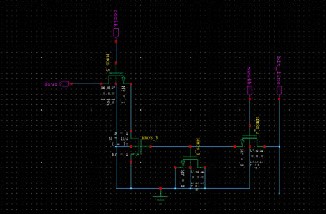
In this we are implementing one by one conceptual architec- tural component required for design of DRAM using Tanner EDA tool. The design flow chart is shown below;
Desig step of architecture in Tanner EDA tool; Step 1:- Open S-edit.
Step 2:- Create a schematic view. Step 3:- Generate symbol of design.
Step 4:- Built a desig using symbolic view. Step 5:- Check for errors in T-spice.
Step 6:- If simulation is successful then check the output wave- form in W-edit.
Step 7:- Save the design.
IJSER © 2013 http://www.ijser.org
International Journal of Scientific & Engineering Research, Volume 4, Issue 7, July-2013 1710
ISSN 2229-5518
Start
Draw the schematic view of architectural component of
DRAM cell
Check for errors
save the schematic & create the symbol | |
Check for errors
save the symbol
&
built the design
start simulation in T-spice
Errors
Errors
write bitline is charged to the value we wish to store in the cell, and the write wordline is strobe. To read from the cell, the read bitline is precharged high and the read wordline is strobe. If a 1 is stored in the cell, transistor T2 turns on and the bitline discharges. The key to fast access times is the gated diode, which is tied to the read wordline. When a 1 is stored in the cell, the diode provides a “boosting” effect to the value at the storage node and temporarily gives it a value close to (and sometimes greater than) Vdd, which allows T2 to turn on quickly and discharge the bitline.
No (More than 3 times)
satisfied with result
No(2 or 3 times)
generate waveform using W -edit
No (More than 3 times)
Satisfied with result
No(2 or 3 times)
Fig. 4: Schematic of 3Transistor 1 Diode DRAM cell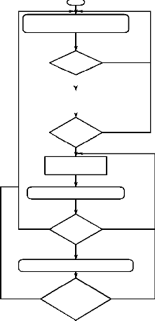
Fig. 3: Three Transistor –One Diode Dram
In light of such problems with the standard 6T SRAM de- sign, researchers are investigating new cell designs that can better withstand process variation. 3T1D cell is one of the pos- sible options proposed by Luk et al. [4]. 3T1D is a DRAM memory cell that, unlike a typical 1T or 1T1C design, provides non-destructive reads and high-speed operation that is com- parable to (and in some cases better than) the standard 6T SRAM cell. 3T1D is also more compact and dissipates less leakage power than the 6T cell [1]. Moreover, it does not suffer from the stability issues that are present in the 6T design: its operation does not rely on the specific device balance, and device mismatch is less likely to cause failure within the cell. Variation only affects the operating frequency of the cell, mak- ing it much more robust to process variation than the 6T de- sign. Figure 4 presents a schematic of a 3T1D cell.
3.1.1 Schematic of 3T-1D Cell
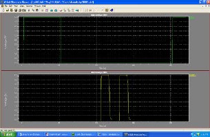
When a 0 is stored in the cell, the capacitance of D1 is smaller and little to no voltage boosting occurs, keeping T2 turned off. Because the 3T1D is a dynamic memory cell, the value at the storage node leaks away as time passes. As this happens, accesses to the cell become slower and slower. Even- tually, this access time becomes so slow that it is no longer comparable to that of the 6T cell. Eventually, the stored value degrades completely. While the fast access times and non- destructive reads of the 3T1D cell produce an attractive 6T cell alternative, 3T1D’s dynamic nature introduces a new issue that SRAM designers need not consider. The input and output of 3T-1D DRAM cell in 1µm Tanner technology is shown be- low.
The schematic view of 3T-1D cell in 1µm technology is shown below. To write to the cell, the write bitline is charged to the value we wish to store in the cell, and the write word- line is strobe. To write to the cell, the write bitline is charged to the value we wish to store in the cell, and the write wordline is strobe. To read from the cell, the read bitline is precharged high and the read wordline is strobe. To write to the cell, the
IJSER © 2013 http://www.ijser.org
Fig.5: Input/output waveform of 3T-1D DRAM Cell
International Journal of Scientific & Engineering Research, Volume 4, Issue 7, July-2013 1711
ISSN 2229-5518
Dynamic random access memory (DRAM) integrated cir- cuits (ICs) have existed for more than twenty-five years. DRAMs evolved from the earliest 1-kilobit (Kb) generation to the recent 1-gigabit (Gb) generation through advances in both semiconductor process and circuit design technology. Tre- mendous advances in process technology have dramatically reduced feature size, permitting ever higher levels of integra- tion. These increases in integration have been accompanied by major improvements in component yield to ensure that overall process solutions remain cost-effective and competitive. Tech- nology improvements, however, are not limited to semicon- ductor processing. Many of the advances in process technolo- gy have been accompanied or enabled by advances in circuit design technology. In this chapter, we introduce some funda- mentals of the DRAM IC, assuming that the reader has a basic background in complementary metal-oxide semiconductor (CMOS) circuit design, layout, and simulation.
In this project we try to design 16-bit DRAM (16 x 1 bit). Schematic diagrams of 3T-1D DRAM cache architecture is shown below. Note that there are 4 address inputs with pin labels R1-R2 and C1-C2. Each address input is connected to an on-chip address input buffer. The input buffers that drive the row (R) and column (C) decoders in the schematic diagram have two purposes; to provide a known input capacitance (CM) on the address input pins and to detect the input address signal at a known level so as to reduce timing errors. The level VTRIP> an idealized trip point around which the input buffers slice the input signals, is important due to the finite transition times on the chip inputs (Figure 6). Ideally, to avoid distorting the duration of the logic zeros and ones, VTRIP should be po- sitioned at a known level relative to the maximum and mini- mum input signal amplitudes. In other words, the reference level should change with changes in temperature, process conditions, input maximum amplitude (Vm), and input mini- mum amplitude (VIL). Having said this, we note that the input buffers used in first-generation DRAMs were simply inverters. Continuing our discussion of the block diagram shown in Fig- ure 6, we see that five address inputs are connected through a decoder to the 16-bit memory array in both the row and col- umn directions. The total number of addresses in each direc- tion, resulting from decoding the2-bit word, is 4. The single memory array is made up of 16 memory elements laid out in a square of 4 rows and 4 columns. Figure 6 illustrates the sche- matic view of this memory array. A memory element is locat- ed at the intersection of a row and a column.
By applying an address of all zeros to the 4 address input pins, the memory data located at the intersection of row 0, RAO, and column 0, CAO, is accessed. (It is either written to or read out, depending on the state of the R/W input and assum- ing that the CE pin is LOW so that the chip is enabled.) It is important to realize that a single bit of memory is accessed by using both a row and a column address. Modern DRAM chips reduce the number of external pins required for the memory address by using the same pins for both the row and column address inputs (address multiplexing). A clock signal row ad- dress strobe (RAS) strobes in a row address and then, on the same set of address pins, a clock signal column address strobe
(CAS) strobes in a column address at a different time.
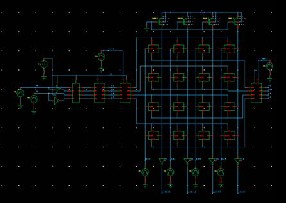
Fig. 6: Schematic of 3Transistor 1 Diode DRAM cell
Also note how a first-generation memory array is orga- nized as a logical square of memory elements. At this point, we don't know what or how the memory elements are made. We just know that there is a circuit at the intersection of a row and column that stores a single bit of data. The input and out- put waveform of 3T-1D DRAM cache architecture in 1µm Tanner technology is shown below.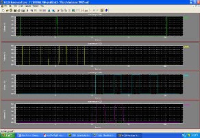
Fig.7: Input/output waveform of 3T-1D DRAM Cache
As continuous technology change for high density memo- ries favors small memory cell sizes, the dynamic RAM cell with a small structure has become a popular choice, where binary data are stored as a charge in a capacitor and the pres- ence or absence of stored charged determine the value of stored bit. The data stored in a capacitor based DRAM cell cannot retain indefinitely, because the leakage current eventu- ally remove or modify the stored data.
We have performed simulations using Tanner EDA tool using two methods. The main purpose of Technology varia- tion is to determine the efficiency, power dissipation and leak- age current of 3T1D DRAM Cells.
IJSER © 2013 http://www.ijser.org
International Journal of Scientific & Engineering Research, Volume 4, Issue 7, July-2013 1712
ISSN 2229-5518
In this second method voltage is kept constant and technol- ogy get changes for same DRAM architecture. The following configuration 1µm, 0.5µm, 0.35µm, 0.25µm & 0.18µm of DRAM cells were designed and analyzed using the Tanner tool. The various configurations were simulated using T-spice.
When applying voltage is kept constant i.e. 5V and tech- nology changes from 1µm to 0.18µm for same 3T- 1D DRAM architecture then we get leakage current which is also called as static current (steady current). Static current is the current that flows between the supply rails in the absence of switching activity.
In this case technology is kept constant in sub threshold region; with input voltage ranges from 5V, 4V, 3V, 2.5V and
1.8V. To establish an impartial testing environment both cir- cuits have been tested on the same input patterns which co- vers all the combination of input stream.
Table 4.6 Voltage Vs Power at 1µm
Table 4.1 Technology Vs Power at 5V
Technology (µm) | Static Current (A) | Power Dissi- pation (mW) |
0.18 | 0.002 | 10 |
0.25 | 0.0018 | 9 |
0.35 | 0.0012 | 6 |
0.5 | 8.85 X 10⁻⁴ | 9 |
1 | 6.54 X 10⁻⁴ | 3.27 |
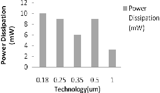
Fig. 8: Technology Vs Power at 5V
According to above graph we can conclude that when ap- plying voltage is 5v at that time 1µm technology is best tech- nology because it gives least power dissipation as compared to other. Also when applying voltage is 5V to 3T-1D DRAM
180nm technology gives maximum power dissipation.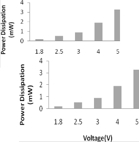
Fig. 9: Voltage Vs Power at 1µm
According to above graph we can conclude that when tech- nology is kept constant at 1µm and applying voltages are 5V,
4V, 3V, 2.5V and 1.8V to 3T-1D DRAM it is observed that 1.8V
gives least power dissipation and 5V gives maximum.
This paper proposes novel process variation in nanotech- nology. Scaling of capacitor in DRAM is critical job. So it can be avoided by capacitorless DRAM out of which 3T-1D is more preferable as compare to 2T-1D DRAM cell. Hence this project proposes to replace on-chip SRAM with 3T-1D DRAM memories, with the specific target of combating process varia- tion. With the help of this project it will possible to get high stability, reduce power requirement and the ability to tolerate performance variation. This approach provides a comprehen- sive solution to many of the issues that will impact on-chip memory design in nanoscale process technologies. This project proposes novel process variation tolerant on-chip memory
IJSER © 2013 http://www.ijser.org
International Journal of Scientific & Engineering Research, Volume 4, Issue 7, July-2013 1713
ISSN 2229-5518
architectures based on a 3T-1D dynamic memory cell. The 3T-
1D DRAM cell is an attractive alternative to conventional 6T
cells for next-generation on-chip memory designs since they
offer better tolerance to process variations that impact perfor-
mance, cell stability, and leakage power.
ABOUT AUTHOR’S
Yogesh Thakre1 received the bache- lor’s degree in Electronics and Tele- communication engineering from HVPM College of Engineering & Technology, Amravati, Maharashtra, India and currently pursuing M. Tech in Electronic System and Communication
[1] X. Liang, R. Canal, G. Wei, and D. Brooks “Replacing 6T SRAMs with
3T1D DRAMs in the L1 data cache to combat process variability”, IEEE Computer Society, Vol.8, No.1:pp.60-68, January-February 2008 .
[2] B. Raj, A. Suman & G. Singh “Analysis of Power Dissipation in DRAM
Cells Design for Nanoscale Memories” International Journal of Infor- mation Technology and Knowledge Management, Vol. 2, No. 2, pp.
371-374 July-December 2009
[3] M. Tien Chang, P. Tsang Huang and W. Hwang “A 65nm Low Power
2T1D Embedded DRAM with Leakage Current Reduction” in 39th IEEE National Science Council and Ministry of Economic Affairs Interna- tional Symposium on Micro architecture, Vol.1, No.12, pp.56-62, July- December 2006.
[4] S. Lin, Y. Kim and F. Lombardi “A 32nm SRAM Design for Low Power and High Stability” IEEE Journal of in Solid-State Circuits, Vo. 42, No.
3, pp. 680 - 688, January-March 2007.
[5] B. Amelifard, F. Fallah “Leakage Minimization of SRAM Cells in a Dual- Vt and Dual-Tox Technology” IEEE Transactions on Very Large Scale Integration (VLSI) Systems, Vol. 16, No. 7, Jun-July 2008.
[6] N. Bhat “ Design and Modeling of Different SRAM’s Based on CNTFET
32nm Technology” International Journal of VLSI design & Communi- cation Systems, Vol.3, No.1, November-February 2012.
[7] J. Koob, S. Ung, B. Cockburn, D. Elliott “Design and Characterization
of a Multilevel DRAM ” IEEE Transactions on Very Large Scale Inte- gration (VLSI) Systems, Vol. 19, No. 9, July- September 2011.
[8] B. Davis “Modern DRAM Architectures” In Proc. 26th Annual Interna- tional Symposium on Computer Architecture, Vol.2, No. 26, pp. 222–
233, July- December 1999.
[9] X. Liang, R. Canal, G. Wei and D. Brooks “Process Variation Tolerant
3T1D-Based Cache Architectures” School of Engineering and Applied
Sciences, Harvard University, Cambridge, vol. 36, no. 4, pp. 658–665,
2001.
[10] S. M. Kang & Y. Leblebici “CMOS Digital Integrated Circuits Analy- sis and Design” 3rd edition TATA McGraw Hill Edition, pp.405-474


from Govt. College of Engineering, Amravati, Maharashtra, India.
Shubhada Thakare2 received the bach- elor ’s and master ’s degree from Amra- vati University. Currently she is an As- sistant Professor at Government College of Engineering, Amravati, Maharashtra,
India with over 14 years of experience in teaching field. Her current areas of research are VLSI and Embedded Systems.

Devendra Chaudhari3 obtained BE, ME, from Marathwada University, Aurangabad and PhD from Indian Institute of Technology, Bombay, Mumbai. He has been engaged in teaching, research for period of about 26 years. Presently he is working as Head, De- partment of Electronics and Telecommunica-
tion Engineering at Government College of Engineering, Amravati. Dr. Chaudhari published research papers and pre- sented papers in international conferences abroad at Seattle, USA and Austria, Europe. His present research and teaching interests are in the field of Biomedical Engineering, Digital Signal Processing and Analogue Integrated Circuits.
IJSER © 2013 http://www.ijser.org