cell grown on Si can theoretically contribute an absolute 5.7% efficiency below Si to a high performance multi junction solar cell system.
International Journal of Scientific & Engineering Research, Volume 4, Issue 6, June-2013 1312
ISSN 2229-5518
Sushma. v.k, Athira sreekumar
M.tech 1st sem students, Department of IT(BMSP&I), RV College of Engineering
Sushmakarjigi@gmail.com, athirasree11@gmail.com
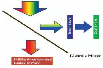
A solar cell is an electrical device that converts light energy directly in to electrical energy by the photovoltaic effect. It is a form of photoelectric cell which when exposed to light can generate an electric current. Photovoltaics continues to be the world’s fastest growing power generation technology due to increasing interests and demands of clean and sustainable energy. Silicon dominates the material supply markets because of its mature technology, ease of fabrication and good efficiency. Optimized high efficiency solar cells can be made in laboratories or manufacturing plants. Multi junction solar cell systems that have a response to a broad range of spectrum is of great interest. In multi junction system sunlight is split by a dichroic mirror, mid energy photons are absorbed by InGap and GaAs solar cells and low energy photons are collected by Si and Si Ge solar cells. Si Ge solar
cell grown on Si can theoretically contribute an absolute 5.7% efficiency below Si to a high performance multi junction solar cell system.
Figure1: A multi-junction solar cell system with standalone Si solar cell and SiGe solar cell.
The multi junction system can be simplified by the replacement by three terminal solar cell.
IJSER © 2013 http://www.ijser.org
International Journal of Scientific & Engineering Research, Volume 4, Issue 6, June-2013 1313
ISSN 2229-5518
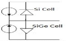
Figure 2: schematic of multi-junction solar cell system with three terminal solar cell.
To further improve solar cells efficiency Si –Si:Ge solar cells have been developed. In this paper, a three terminal Si-Si:Ge tandem solar cell consisting of a top silicon solar cell and bottom Si:Ge solar cell sharing the same base which can take the advantage of both Si solar cell and Si:Ge solar cell and overcome the current mismatch effect and optic loses between them, will be reported .
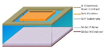
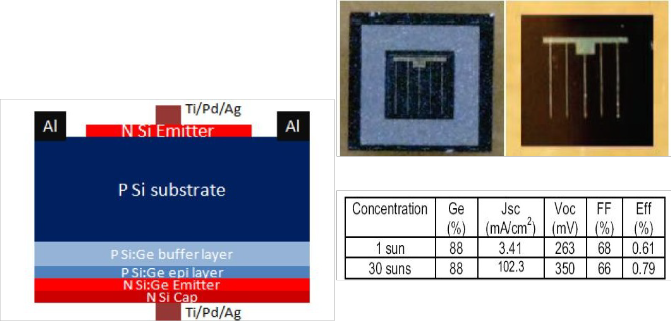
A three terminal Si-Si:Ge solar cell is an integration of standalone transparent silicon solar cell and a low band gap Si: Ge solar cell. The basic structure of the Si-Si:Ge tandem solar cell is illustrated in Figure 3. The top cell is a silicon solar cell with a band gap of 1.12 eV. Contacts for the base and emitter of silicon solar cell is on the same side. Al contact for the silicon solar cell is also shared by the bottom Si:Ge solar cell with approximately 88% Ge concentration. The current flow of the three terminal solar cell is as follows. The holes generated will flow towards the common base and be collected by the base Al contact. Electrons generated by the silicon cell will flow towards the upper (Si) emitter, and electrons generated in the Si: Ge solar cell will flow towards the bottom (Si:Ge) emitter. The equivalent circuits of the ideal solar cell consist of two PN junctions sharing common base. It is shown in Figure 4
Figure 3: schematic vertical cross section of Si-Si:Ge tandom solar cell.
Figure 4: Equivalent circuit of Si-Si:Ge tandom solar cell.
To improve the performance of three terminal Si- Si:Ge solar cells, three groups of solar cells were fabricated. Their fabrication process test results are reported as follows..
A. Group one fabrication and performance
This is the first time fabrication of the three terminal Si-Si:Ge monolithic tandem solar cells. The silicon solar cell emitters were diffused in our own diffusion furnace, which is capable to form very good emitters and the sheet resistance was about 45Ω/sq. The silicon solar cell performance in the three terminal Si-Si:Ge monolithic tandem solar cells is shown in Table 1.
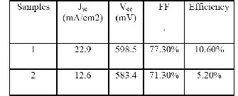
Table 1.Silicon solar cells performance in the first group
In the first group silicon wafers were POCI3 diffused to form N type emitter ,then the backside diffused region was etched so that the epitaxial layers were grown on P type Si substrate. Testing was performed outdoors. The Si solar cell and Si Ge solar cells were tested separately. To measure the performance of the silicon solar cell, in a three terminal solar cell structure, the Si solar cell faces towards the sun directly, and its emitter contact and the Al common base contact were connected to the IV tester. While the Si:Ge solar cell emitter was floating Table 2 shows the measured data in sun.
IJSER © 2013 http://www.ijser.org
International Journal of Scientific & Engineering Research, Volume 4, Issue 6, June-2013 1314
ISSN 2229-5518
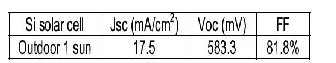
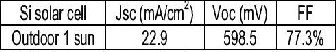
Table 1: summary of si solar cell performance in one group.
The performance of IV curve in this sample was not good. There was a problem of contact between Si :Ge and metal. All the curves behaved like Si and Ge PN junction were connected in series. The back side of the N type diffused silicon layer was not etched away completely before P and N type Si:Ge epitaxial layers were grown on it, so there were two PN junctions on the back side. A second design was developed to eliminate the problem based on epitaxial silicon emitter.
B. Group two fabrication and performance.
The emitter of the secong group solar cells with a thickness of 1 um and a doping density of 5x1017 cm-3 were grown on a P type silicon substrate. Next Si:Ge epitaxial layers were grown on the other side of substrate including a 5um 86.3% . Ge P type Si:Ge base with doping density around 1017cm-3, a 1um 86.3% Ge n type Si:Ge layer with doping density 1017cm-3 and a 200nm n+ silicon gap.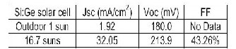
Table 3: Summary of Si solar cells in group 2
Table 4: Summary of Si:Ge solar cells in group 2.
The performance of the silicon solar cell is fair .Compared to the silicon solar cell in group one, the diffusion emitter is a better choice. The performance of Si:Ge was a little bit surprise, because there was a lot of scratches on the Si:Ge epitaxial layer after growth which replicates any defect on the surface of silicon wafer. The emitter growth on this Si:Ge solar cell is good. The third group was fabricated to improve the performance of Si:Ge solar cells.
Figure 6: Actual Si solarcell(left)and Si:Ge solar cell(right)
Table 5. Measured data under 30 suns.
Figure 5. Si emitter and Si:Ge epitaxial layers
The rest fabrication are same as in group one and these solar cells were tested in the same way as described above and the tested results are shown in Tables 3and 4
C. Group three fabrication and performance
Silicon solar cells performance is not good due to the rough surface and low quality of silicon substrate on which N type silicon emitter was grown. the silicon epitaxial layer was grown on the unpolished surface of silicon substrate. The 0.5 um thin silicon emitter will duplicate the shape of the
IJSER © 2013 http://www.ijser.org
International Journal of Scientific & Engineering Research, Volume 4, Issue 6, June-2013 1315
ISSN 2229-5518
rough surface, growth across the surface is not uniform, so good growth cannot be guaranteed. Also rough surface leads to more surface area which means more recombination across surface. To find out the quality of silicon substrate, an experiment was designed to find the lifetime of both emitter and base. Lifetime of emitter and base are 3.3 us and 14.3 us respectively. Low lifetime means high recombination, short diffusion length and low collection probability. Si:Ge solar cells performance is improved as expected . While its performance can be further improved, since the best mono-junction Si:Ge solar cell made by Yi with similar structure has a Voc of 263mV, Jsc of
3.41mA/cm2 and FF 61% below silicon filter under one sun. To make a good 3 terminal Si-Si:Ge solar cells, a good silicon substrate has to be selected, polished, high lifetime FZ material, resistivity close to 0.2Ω-cm. Polished substrate can provide good growth platform for Si:Ge epitaxial layer. Diffusion is a better choice to form PN junction once high performance diffusion is accessible, and thermal oxidation can be done right after diffusion. High open ,circuit voltage can achieved at this moment . The three terminal Si-Si:Ge solar cell was grown on a polished side of a substrate. The emitter of the silicon solar cell is 0.5 um and a doping density of
5x1015cm-3 and 88% Ge and N type Si :Ge silicon solar cell whose emitter layer is 1um thick .
This work focuses on the design and fabrication of three terminal Si-Si:Ge monolithic tandem solar cells. Three terminal Si-Si:Ge monolithic tandem solar cell combines a transparent silicon solar cells and a high concentration Ge Si:Ge solar cell The first fabrication yielded good silicon solar cells with a Jsc of 22.9 mA/cm2, Voc of 598.5mV and FF of
77.3%, though the Si:Ge solar cell was not good . In the second group both silicon solar cells and Si:Ge solar cells had good performance., Si solar cell with a Jsc of 17.5mA/cm2, Voc of 583.3mV, FF of
81.8%, Si:Ge solar cell with Jsc of 1.92 mA/cm2, Voc of 180mV below silicon filter at one sun was achieved. The third group improved the Si:Ge solar cells performance to Jsc of 3.26mA/cm2, Voc of
189mV below silicon filter under one sun. This
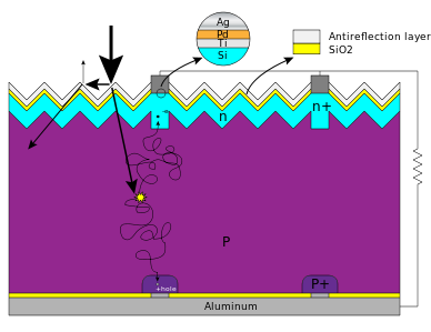
work demonstrates that this structure can achieve higher potential efficiency, easier fabrication process ,lower cost, lower optic loses, less surface recombination because of lesser surface areas ,than transparent silicon solar cells and Si Ge solar cells and avoid mismatch that exist in two terminal multijunction solar cells. To further improve the performance of three terminal Si-Si:Ge solar cell, the following can be optimized including material selection, fabrication process, and optics implementation. A good silicon substrate has to be selected which directly influences silicon solar cells performance. High lifetime FZ material with resistivity close to 0.2Ω-cm. High lifetime means less bulk recombination and higher carrier collection probability resulting in higher voltage as well as higher current density. 0.2Ω-cm is an optimized resistivity, which can lead to high potential voltage but also higher transparency of infrared light. Polished surface is a better platform for epitaxial growth than a rough surface ,growth happens on polished side if growth layers are in the range of nanometers. Optics including antireflection (AR) coatings and pyramids are powerful tools to increase light generated current, since they can trap light within solar cells. AR coatings and pyramids can minimize the reflection at front surface and maximize the reflection at back surface, change pathways of photons inside solar cells, so that light will be trapped within solar cells which allow more absorption. A back side inverted pyramids with SiO2 as mirror in mono-junction Si:Ge solar cell can increase the optic path length up to 17 time solar cells physical thickness.
IJSER © 2013 http://www.ijser.org
International Journal of Scientific & Engineering Research, Volume 4, Issue 6, June-2013 1316
ISSN 2229-5518
Figure 7. Configuration of improved 3T solar cell.
A Si solar cell and a Si:Ge solar cell can be integrated into a three terminal Si-Si:Ge solar cell, which can be applied in the multi-junction solar cell system to replace the former independent two solar cells.This can simplify module, improving the performance and reduce its cost. Better performance of 3 terminal Si-Si:Ge solar cells will achieved by improving structure design, fabrication and application of light trapping optics.
[1] Lu, Wang, etc., “Three Terminal Si-Si:Ge
Solar Cell”. 37th IEEE PVSC, Seattle, USA.
[2] Christopher, Kerestes. “Design, Fabrication and Analysis of Transparent Silicon Solar Cells,”. Ph.D. Thesis, University of Delaware,
2010.
[3] A.G. Martin. “The path to 25% silicon solar cell efficiency: history of silicon cell evolution”. Progress in Photovoltaics: Research and Applications 17 (2009), pp. 183–
189 .
[4] Khalid Said, et al. “Design, Fabrication,and
analysis of Crystalline Si-SiGe Heterostructure Thin film solar cell IEEE TRANSACTIONS ON ELECTRON DEVICES, VOL. 46, NO.
10, OCTOBER 1999.
[5] Allen Barnett, et.al. “Very High Efficiency Solar Cell Modules”, Prog. Photovolt: Res. Appl. 17 (2009) 75- 83.
[6] CB Honsberg, AM Barnett, D Kirkpatrick.
"Nanostructured Solar Cells For High Efficiency Photovoltaics," Photovoltaic Energy Conversion, IEEE 4th World Conference, May
2006, Hawaii, USA .
[7] Shockley, W., W. T. Read, "Statistics of the Recombinations of Holes and Electrons,", Physical Review, vol. 87, no. 5, pp. 835, 1952.
[8] Yi Wang, “Design, Fabrication, and Analysis of Ge:Si Solar Cells”, Ph.D. Thesis, University
of Delaware, 2010.
[9] Schmid, P.E., “Optical Absorption in Heavily
Doped Silicon,”, Physical Review B, Vol. 23, No. 10, p. 5531-5536, 198.
[10] Clugston, Donald A. and Basore, Paul A., “Modeling Free-Carrier Absorption in Solar
Cells”, Progress in Photovoltaics: Research and
Applications,Vol.5,p.229-236,1999.
IJSER © 2013 http://www.ijser.org