International Journal of Scientific & Engineering Research, Volume 4, Issue 6, June-2013 178
ISSN 2229-5518
A Novel Cache Architecture For Multicore
Processor Using Vlsi
Sujitha .S, Anitha .N
Abstract— Memory cell design for cache memories is a major concern in current Microprocessors mainly due to its impact on energy consumption, area and access time. Cache memories dissipate an important amount of the energy budget in current microprocessors. An n-bit cache cell, namely macrocell, has been proposed. This cell combines SRAM and eDRAM technologies with the aim of reducing energy consumption while maintaining the performance. The proposed M-Cache is implemented in processor architecture and its performance is evaluated. The main objective of this project is to design a newly modified cache of Macrocell (4T cell). The speed of these cells is comparable to the speed of 6T SRAM cells. The performance of the processor architecture including this modified-cache is better than the conventional Macrocell cache design. Further this Modified Macrocell is implemented in Mobile processor architecture and compared with the conventional memory. Also a newly designed Femtocell is compared with both the macrocell and Modified m-cache cell.
Index Terms— Femtocell. L1 cache, L2 cache, Macrocell, Modified M-cell, UART.
—————————— ——————————
1 INTRODUCTION
PROCESSORS are generally able to perform operations on operands faster than the access time of large capacity main memory. Though semiconductor memory which can operate at speeds comparable with the operation of the processor exists, it is not economical to provide all the main memory with very high speed semiconductor memory. The problem can be alleviated by introducing a small block of high speed memory called a cache between the main memory and the processor. The idea of cache memories is similar to virtual memory in that some active portion of a low-speed memory is stored in duplicate in a higher speed cache memory. When a memory request is generated, the request is first presented to the cache memory, and if the cache cannot respond, the request is then presented to main memory. The difference between cache and virtual memory is a matter of implementation; the two notions are conceptually the same because they both rely on the correlation properties observed in sequences of address references. Cache implementations are totally different from virtual memory implementation because of the speed requirements of cache.
————————————————
• Sujitha .S is currently pursuing masters degree program in
communication systems in Mount Zion College of Engineering,Pudukottai, India ,PH-8973518996. E-mail:srsujalsekar@gmail.com
• Anitha .N is currently working as Assistant professor in the department of electronics and communication engineering in Mount Zion College of Engineering, Pudukootai, India. E-mail:anis.anitha88@mail.com
The cache operation is that when the CPU requests contents of memory location, it first checks cache for this data, if present, get from cache (fast), if not present, read required block from main memory to cache. Then, deliver from cache to CPU. Cache includes tags to identify which block of main memory is in each cache slot. In today’s systems, the time it takes to bring an instruction (or piece of data) into the processor is very long when compared to the time to execute the instruction.
Cache memories occupy an important percentage of the overall die area. A major drawback of these memories is the amount of dissipated static energy or leakage, which is proportional to the number of transistors used to implement these structures. Furthermore, this problem is expected to aggravate further provided that the transistor size will continue shrinking in future technologies. Cache memories dissipate an important amount of the energy budget in current microprocessors. This is mainly due to cache cells are typically implemented with six transistors. To tackle this design concern, recent research has focused on the proposal of new cache cells. An -bit cache cell, namely macrocell, has been proposed in a previous work.
Generally cache memories are implemented using SRAM. The main reason is cost. SRAM is several times more expense than DRAM. Also, SRAM consumes more power and is less dense than DRAM. Now that the reason for cache has been established, let look at a simplified model of a cache system. SRAM and DRAM cells have been the predominant technologies used to implement memory cells in computer systems, each one having its advantages and shortcomings. SRAM cells are faster and require no refresh since reads are not destructive. In contrast, DRAM cells provide higher density and minimal leakage energy since
IJSER © 2013 http://www.ijser.org
International Journal of Scientific & Engineering Research, Volume 4, Issue 6, June-2013 179
ISSN 2229-5518
there are no paths within the cell from Vdd to ground. Recently, DRAM cells have been embedded in logic-based technology, thus overcoming the speed limit of typical DRAM cells.
Typically, 1T1C DRAM cells were too slow to implement processor caches. However, technology advances have recently allowed to embed DRAM cells using CMOS technology [1]. An embedded DRAM cell (eDRAM) integrates a trench DRAM storage cell into a logic-circuit technology. In this way, the read operation delays can come out to have similar values than SRAM. As a consequence, recent commercial processors use eDRAM technology to implement L2 caches [2, 3]. Despite technology advances, an important drawback of DRAM cells is that reads are destructive, that is, the capacitor loses its state when it is read. In addition, capacitors lose their charge along time, thus they must be recharged or refreshed. To refresh memory cells, extra refresh logic is required which in turn results not only in additional power consumption but also in availability overhead.
An n-bit memory cell (from now on macrocell) with one SRAM cell and eDRAM cells designed to implement n-way set-associative caches [4]. SRAM cells provide low latencies and availability while eDRAM cells allow reducing leakage consumption and increasing memory density. Results showed that a retention time around 50 K processor cycles was long enough to avoid performance losses in an L1 cache memory macrocell-based data cache.
The conventional macrocell reduces power consumption when compared to general SRAM cache memory. The problem of leakage energy is the main concern in this macrocell. However these macrocell has impact on performance and occupies more area since six transistors (6T SRAM) are used. Hence a newly modified M-cell is designed to overcome these drawbacks. The new M-cell consists of four transistors (4T) which does not include two transistors connected to Vdd. This cell offers an easy method for DRAM implementation in a logic process production, especially in embedded systems.
This work consists of two parts: to implement the macrocell in a processor architecture and corresponding area, speed and power is measured. Then, to design a new cell Modified Macrocell in order to overcome the drawback in conventional Macrocell and analyze the performance in this cell.
2 MACROCELL CACHE MEMORY
The cache memory cells have been typically implemented in microprocessor systems using static random access memory (SRAM) technology because it provides fast access time and does not require refresh operations. SRAM cells are usually implemented with six transistors (6T cells). The major drawbacks of SRAM caches are that they occupy a significant percentage of the overall die area and consume an important amount of energy, especially leakage energy which is proportional to the number of transistors. Furthermore, this problem is expected to aggravate with future technology generations that will continue shrinking the transistor size.

DRAM cells have been considered too slow for processor caches. Nevertheless, technology advances have recently allowed to embed DRAM cells using CMOS technology [1]. An embedded DRAM cell (eDRAM) integrates a trench DRAM storage cell into a logic-circuit technology and provides similar access delays as those presented by SRAM cells. As a consequence, some recent commercial processors use eDRAM technology to implement last-level caches [3], [4].
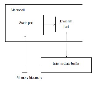
Fig. 1. Macrocell Block Diagram
In [5], it has been proposed an -bit memory cell (from now on macrocell) with one SRAM cell and n-1 eDRAM cells designed to implement n-way set-associative caches. SRAM cells provide low latencies and availability while eDRAM cells allow reducing leakage consumption and increasing memory density. Results showed that a retention time around 50 K processor cycles was long enough to avoid performance losses in an L1 macrocell- based data cache (from now on M-Cache).
IJSER © 2013 http://www.ijser.org
International Journal of Scientific & Engineering Research, Volume 4, Issue 6, June-2013 180
ISSN 2229-5518
2.1 Macrocell Internals
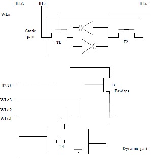
The main components of an n-bit macrocell are a typical SRAM cell,n-1 eDRAM cells and bridge transistors that communicate SRAM with eDRAM cells. Fig. 1 depicts an implementation of a 4-bit macrocell. The SRAM cell comprises the static part of the macrocell. Read and write operations in this part are managed in the same way as in a typical SRAM cell through the bitline signals (BLs and
/BLs).The dynamic part is formed by n-1eDRAM cells (three in the example). Each eDRAM cell consists of a capacitor and an NMOS pass transistor, controlled by the corresponding word line signal (WLdi). Wordlines allow each capacitor to be accessed through the corresponding bitline (BLd). Read and write operations perform as in a conventional eDRAM cell through the corresponding pass transistor.
The bridge transistors connect the SRAM cell to each eDRAM cell and are controlled by the corresponding static to dynamic signal (s2di). Each bridge transistor acts as an unidirectional path to transfer data from the SRAM cell to a given eDRAM cell without using intermediate buffers. These transfers are referred to as internal since no bitline is involved.
2.2 Internal transfers
Internal transfers provide a fast and low energy consumption mechanism to copy data stored in the SRAM cell to the dynamic part. The idea is to keep the data most recently used (MRU) by the processor always in the SRAM cell. Previous works [6] have shown that the MRU line in each cache set use to be accessed with a much higher probability than the remaining ones (for instance, 92.15% of the accesses in a 16 kB-4 way L1). Therefore, keeping the MRU data in the SRAM cell might provide energy benefits because SRAM reads are non-destructive. The remaining data is stored in the dynamic part which loses their state when the retention time expires. This will happen if this data is not referenced for long.
Internal transfers are triggered when the data required by the processor is not stored in the SRAM cell (SRAM miss). In this case, the content of the SRAM cell is copied to an eDRAM cell and replaced by the referenced data. To do so, the cache controller manages a swap operation in three sequential steps
as shown in Fig. 2. First, the data stored in the dynamic part
is written to an intermediate buffer, and then an internal
transfer is performed to copy the data from the static to the dynamic part by switching on the corresponding bridge transistor and after that, the data referenced by the processor is written to the static part. This data can come
either from the intermediate buffer (i.e., on an eDRAM hit) or from a lower level of the memory hierarchy (i.e., on a cache miss).
3 PROCESSOR ARCHITECTURE
Modern computers are truly marvels. They are an indispensable tool for business and creativity. Despite this, most people have no clear idea what goes on inside their computers. The conceptual design of a general-purpose computer and the key technologies inside the processor and how they relate to other system components are described.

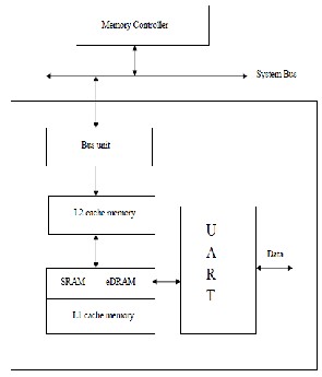
Fig. 2. Processor Architecture
All computers run using very low-level commands which do some very basic functions, such as reading data, writing data, and address jumping, and basic arithmetic The processor architecture includes the main component CPU (UART) processor, a main memory generally SRAM, L1 cache unit and L2 cache unit. The UART processor is the main unit for processing the data. Closest to the processor is Level 1 (L1) cache. This is very fast memory used to store data frequently used by the processor. Level 2 (L2) cache is just off-chip, slower than L1 cache, but still much faster than main memory. L2 cache is larger than L1 cache and used for the same purpose.
Main memory is very large and slower than cache and is used, for example, to store a file currently being edited in Microsoft Word. Most systems have between 1GB to 4GB of main memory compared to approximately 32KB
IJSER © 2013 http://www.ijser.org
International Journal of Scientific & Engineering Research, Volume 4, Issue 6, June-2013 181
ISSN 2229-5518
of L1 and 2MB of L2 cache. Finally, when data isn’t located in cache or main memory the system must retrieve it from the hard disk, which takes exponentially more time than
reading from the memory system.
3.1 Description
Data retrieved from system memory traverses the memory controller, the system bus, the Level 2 cache, and the Level
1 caches. The L1 data cache interfaces directly to the execution unit while the L1 instruction cache interfaces to the instruction fetch/decode stage. The close proximity of the L2 and L1 caches to the instruction execution pipeline significantly increases performance.
Performance-analysis tools are available to measure the cache hit rate, which indicates the percentage of time the execution unit is fed from the cache. Cache hit rate is a measure of cache efficiency, and it often correlates to the application program's reference locality, which refers to the degree to which a program's memory accesses are limited to a relatively small number of addresses.
Conversely, a program that accesses a large amount of data from scattered addresses is less likely to use cache memory efficiently. For example, a packet-processing application that's performing TCP reassembly on a large number of TCP flows is likely to access a large amount of data over many memory locations. This results in a lower locality of reference than an application that's performing TCP reassembly on a smaller number of TCP flows.
4 PROPOSED ARCHITECTURE
4.1 Modified M-cell memory
The modified Macrocell consists of four transistors (4T) RAM cells. 4T cells are approximately as fast as 6T SRAM cells, but do not have connections to the gate voltage (Vdd).
Rather, the 4T cell is charged upon each access, whether read or write, and slowly leaks the charge over time. This modified cell offers area savings and leakage power savings when compared to the conventional Macrocell.
The input voltage applied to this cell is limited. Hence is the total power is reduced and the leakage power across the transistor seems to be low when compared to the conventional M-cell cache unit. 4T cells are about as fast as
6T cells, but they do not store charge indefinitely. Rather,
the charge gradually leaks away at a rate that is a function of the cell’s specific design as well as the current operating temperature. This caps the amount of leakage energy that an unused cell can dissipate. The area benefits of 4T cells stem from the fact that power and ground lines need not
stripe vertically down the array. 4T cells are especially applicable to on-chip structures whose data is both transient and predictive.

Fig. 3. Modified Macrocell cache memory
4.2 FEMTOCELL Cache Memory
The modified macrocell is made up of four transistors hence better than Macrocell. Eventhough this Modifird m- cell still has impact on power consumption and more leakage power hence a new cell named Femtocell is designed to overcome the drawbacks in both the conventional and modified cell.
This Femtocell seems to be occupy less memory space
and consumes low power. These design can be implemented in the mobile processor and their performance can be compared .
IJSER © 2013 http://www.ijser.org
International Journal of Scientific & Engineering Research, Volume 4, Issue 6, June-2013 182
ISSN 2229-5518
5 MOBILE PROCESSOR ARCHITECTURE


600
500
400
300
200
100
0
Macrocell
Based Cache
Modified Macrocell Cache
Femtocell
LUT FLIPFLOPS
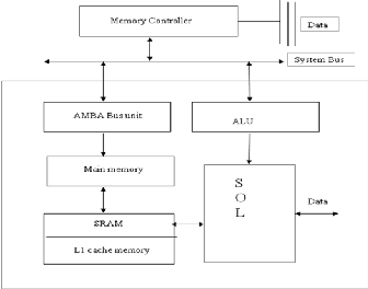
Fig. 4. Mobile Processor Architecture
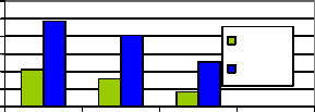
Fig. 5. Comparison chart-Area Usage
5.1 DESCRIPTION
The mobile processor architecture consists of SOL processor, an AMBA bus unit, main memory, An Arithmetic and Logic unit, a SDRAM cache memory and memory controller.
The Macrocell as well as the Femtocell can be
implemented in cache memory unit and their comparison can be compared with the SDRAM.
6 SIMULATION RESULTS
The functional simulation of the proposed architecture has been justified by using Verilog HDL. The propose

600
500
400
300
200
100
0
Ma croce ll
Ba s e d Ca che
Modifie d Ma croce ll Ca che
Femtoce ll
Ca che
LUT
FLI PFLOPS
architecture are verified by the XILINX ISE software. The proposed architecture is further validated in TINA 7 software.
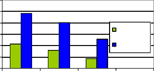
Fig. 5. Comparison Chart – Speed & Power
TABLE 2
Leakage power measured for different cache cells
TABLE 1
Comparison Results
Methodology | Area | Speed | Power |
Macro-Cell Based Cache | Flip flop(486) LUT(213) | 109.74MHz | 49.92nW |
Modified Macrocell Based Cache | Flip flop(405) LUT(158) | 123.70MHz | 35.64nW |
IJSER © 2013 http://www.ijser.org
International Journal of Scientific & Engineering Research, Volume 4, Issue 6, June-2013 183
ISSN 2229-5518
7 CONCLUSION
The L1 Macrocell cache memory is designed and verified. This M-cell is implemented in the processor architecture and the overall area utilization speed and power is measured. These are analyzed using XILINX software. A newly modified structure of conventional M-cell is designed and its corresponding functionality including power and leakage power is measured. The output is verified in TINA software. A newly designed Femtocell is also compared with the above two cells.
The total power consumption for Modified Macrocell seems to be low when compared to Conventional Macrocell and their corresponding leakage power is also low. Whereas the performance of Femtocell seems to be better than the other two Macrocell cache memory. These cache cells can also be implemented in the mobile processor architecture and their performance can be analyzed.
REFERENCES
[1] Alejandro Valero, Julio Sahuquillo, Member, IEEE, Vicente Lorente, Salvador Petit, Member, IEEE,Pedro Lopez, Member, IEEE, and José Duato,(2012),“Impact on Performance and Energy of the RetentionTime and Processor Frequency in L1Macrocell-Based Data Caches”,IEEE Transactions On Very Large Scale Integration (VlSI) Systems, vol. 20, no. 6
[2] Flautner .K, Kim .N.S, Martin .S, Blaauw .D, and Mudge .T, (2002) “Drowsy caches: Simple techniques for reducing leakage power,” in Proc. 29th Annu. Int. Symp. Comput. Arch., pp. 148–157
[3] Hu .Z, Juang .P, Diodato .P, Kaxiras .S, Skadron .S, Martonosi
.M, and Clark .D.W, (2002),“Process variation tolerant 3T1D- Based cache architectures,” in Proc. Int. Symp. Low Power Electron. Design, pp. 52–55
[4] Jernej Barbic,”Multi-core architectures”,15-213, Spring 2007
May 3, 2007
[5] Kaxiras .S, Hu .Z, and Martonosi .M, (2001) “Cache decay: Exploiting generational behavior to reduce cache leakage power,” in Proc. 28th Annu. Int. Symp. Comput. Arch., pp.
240–251
[6] Kirihata .T, Parries .P, Hanson D. R, Kim .H, Golz .J, Fredeman .G, Rajeevakumar .R, Griesemer .J, Robson .N, Cestero .A, Khan .B. A, Wang .G, Wordeman .M, and Iyer .S. S (2005), “An 800-MHz embedded DRAM with a concurrent refresh mode,” IEEE J. Solid-State Circuits, vol. 40, no. 6, pp.
1377–1387
[7] Matick .R. E and Schuster .S. E, (2005), “Logic-based eDRAM:
Origins and rationale for use,” IBM J. Res. Develop., vol. 49, no. 1, pp. 145–165
[8] S. Petit, J. Sahuquillo, J. M. Such, and D. Kaeli, “Exploiting temporal locality in drowsy cache policies,” in Proc. 2nd Conf. Comput. Frontiers, 2005, pp. 371–377
[9] Powell .M, Yang .S. H, Falsafi .B, Roy .K, and Vijaykumar
.T.N, (2000), “Gated-Vdd: A circuit technique to reduce leakage in deep-submicron cache memories,” in Proc. Int. Symp. Low Power Electron. Design, pp. 90–95
[10] Sinharoy .B, Kalla .R. N, Tendler .J. M, Eickemeyer .R. J, and Joyner .J. B, (2005), “POWER5 system microarchitecture,” IBM J. Res. Develop., vol. 49, no. 4/5, pp. 505–521
[11] Valero .A, Sahuquillo .J, Petit .S, Lorente .V, Canal .R, López
.P, and Duato .J, (2009), “An hybrid eDRAM/SRAM macrocell to implement first-level data caches,” in Proc. 42th Annu. IEEE/ACM Int. Symp. Microarch., pp. 213–221
[12] Weste .N and Harris .D, CMOS VLSI Design: A Circuits and
Systems Perspective. Boston, MA: Addison-Wesley, 2010
[13] X. Wu, J. Li, L. Zhang, E. Speight, R. Rajamony, and Y. Xie, “Hybrid cache architecture with disparate memory technologies,” in Proc. 36th Annu. Int. Symp. Comput. Arch.,
2009, pp. 34–45
[14] S. Schuster, L. Terman, and R. Franch. A 4-device cmos static ram cell using sub-threshold conduction. In Symposium on VLSI Technology, Systems, and Applications, 1987
[15] K. K. Parhi, VLSI Digital Signal Processing Systems: Design and
Implementation, New York: John Wiley & Sons, 1999.
[16] D. Brooks, V. Tiwari, and M. Martonosi. Wattch: A Framework for Architecture-Level Power Analysis and Optimizations. In Proc. ISCA-27, ISCA 2000.
IJSER © 2013 http://www.ijser.org
