The research paper published by IJSER journal is about A New High Speed - Low Power 12 Transistor Full Adder Design with GDI Technique 1
ISSN 2229-5518
A New High Speed - Low Power 12 Transistor
Full Adder Design with GDI Technique
Shahid Jaman, Nahian Chowdhury, Aasim Ullah, Muhammad Foyazur Rahman
Abstract— The low power and high performance 1-bit full adder cell is proposed in this paper. The Gate Diffusion Input (GDI) technique has been used for the simultaneous generation of XOR and XNOR functions. The resulting full adder circuit is realized using of the 12 transistors, while having full voltage-swing in all circuit nodes. By optimizing the transistor, size in each stage the power and delay are minimized. The full adder are simulated with PSPICE which shows that the new full adder circuit has the lowest power and delay over a wide range of voltages among several low-power adder cells of different CMOS logic styles.
Index Terms— Full Adder, GDI Technique, Low Power, Power-Delay-Product (PDP)
—————————— ——————————
ECENTLY building low-power VLSI systems has emerged as highly in demand because of the fast growing technologies in mobile communication and computation.
The battery technology does not advance at the same rate as the microelectronics technology. There is a limited amount of power available for the mobile systems. So designers are faced with more constraints: high speed, high throughput, small silicon area, and at the same time, low-power consumption. So building low power, high performance adder cells are of great interest [1].
The goal of this paper is designing a high speed and so low- power full adder cell with the GDI technique. This technique that was recently developed and presented in [2], proposes an efficient alternative for logic design in standard CMOS tech- nologies.
The rest of this paper is organized as follow; in section II, we review the previous designs of 1-bit full adder cells. In section III, the GDI technique and implementation method of XOR and XNOR functions using this technique are presented. In section IV, we present the new design of proposed low- voltage and low-power 1-bit full adder circuit. In section V, we describe simulation results and compare the performance of the new full adder with other circuits. Finally, we make con- clusions in section VI.
There are different types of CMOS full adder. This section re- viewed some 1-bit full adder cell, which has proposed by dif- ferent scientist and full adder researcher. This new design is compared with them.
————————————————
![]() Shahid Jaman is with the dept. of EEE in Ahsanullah University of science and Technology (AUST), Bangladesh, Email: sha- hid_jaman_aust@yahoo.com
Shahid Jaman is with the dept. of EEE in Ahsanullah University of science and Technology (AUST), Bangladesh, Email: sha- hid_jaman_aust@yahoo.com
![]() Nahian Chowdhury is with the dept. of EEE in Ahsanullah University of
Nahian Chowdhury is with the dept. of EEE in Ahsanullah University of
Science and Technology (AUST), Bangladesh, Email: nahian.eee@live.com
![]() Aasim Ullah is with the dept. of Electrical Power Engineering in Norwe- gian University of Science & Technology, (NTNU). Email: aasim@kth.se
Aasim Ullah is with the dept. of Electrical Power Engineering in Norwe- gian University of Science & Technology, (NTNU). Email: aasim@kth.se
![]() Mummad Foyazur Rahman is with the dept. of EEE in American Interna-
Mummad Foyazur Rahman is with the dept. of EEE in American Interna-
tional University Bangladesh. Email: foyaz.aiub@yahoo.com
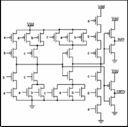
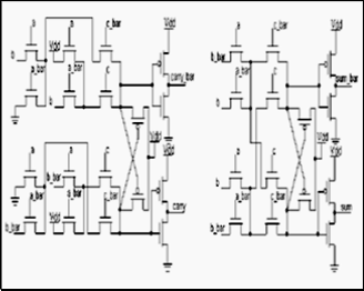
Some designs of adder cells can be found in the figures 1 to 5. These five different adder cells are simulated in 0.18 μm CMOS technology and tested separately. All these cells are optimum in power dissipation and Power delay product (PDP). The conventional adder shown in figure 1 is imple- mented with 28 Transistors in CMOS technology. Convention- al adder circuits do not function well below 1 V supply [3]. Figure 2 shows the Complementary Pass-transistor Logic (CPL) adder. Among the pass transistor logic styles, CPL has the best performance and the lowest power delay product [4]. The Transmission Function full Adder (TFA), which is shown in figure 3, uses 16 transistors. Pull-up and pull-down logic is used to drive the load the same as the complementary pass logic [18]. Figure 4 shows the Transmission Gate full adder (TG). TG adder includes 20 transistors, and generates a+b and its complement to produce the sum and carry signals. It uses complementary input signals (a,b,c) as the complementary CMOS full adder [6,7]. This full adder uses only 14 transistors to make the adder function. The circuit occupies less area in comparison with other CMOS full adder cells [7]. At end, another full adder with 26 transistors is presented in figure 6 [8].
IJSER © 2012
The research paper published by IJSER journal is about A New High Speed - Low Power 12 Transistor Full Adder Design with GDI Technique 2
ISSN 2229-5518


Gate-Diffusion-Input (GDI) method is based on the use of a simple cell as shown in figure .2. At a first glance the basic cell reminds the standard CMOS inverter, but there are some im- portant differences:
1) GDI cell contains three inputs – G (common gate input of
IJSER © 2012
The research paper published by IJSER journal is about A New High Speed - Low Power 12 Transistor Full Adder Design with GDI Technique 3
ISSN 2229-5518
NMOS and PMOS), P (input to the source/drain of PMOS), and N (input to the source/drain of NMOS).
2) Bulks of both NMOS and PMOS are connected to N or P respectively, so it can be arbitrarily biased at contrast with CMOS inverter. It must be remarked, that not all the functions are possible in standard P-Well CMOS process, but can be suc- cessfully implemented in Twin-Well CMOS.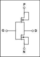
Table I shows how a simple change of the input configuration of the simple GDI cell corresponds to very different Boolean functions. Most of these functions are complex (6-12 transis- tors) in CMOS, as well as in standard PTL implementations, but very simple (only 2 transistors per function) in GDI design method.
N | P | G | D |
‘0’ | B | A | A`B |
B | ‘1’ | A | A`+B |
‘1’ | B | A | A+B |
B | ‘0’ | A | AB |
C | B | A | A`B+AC |
‘0’ | ‘1’ | A | A` |

XOR and XNOR functions are the key variables in adder equations. If the generation of them is optimized, this could greatly enhance the performance of the full adder cell. In this new cell, we have used the GDI technique for generating of XOR and XNOR functions. It uses only six transistors sepa- rately to generate the basic XOR and XNOR functions, as shown in Figure 3.
A one-bit binary full adder takes three one-bit inputs: A, B and![]()
![]()
Cin and generate sum and carry.
The goal of this paper is to design a high speed and low power full adder cell with the GDI technique.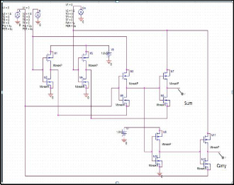
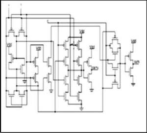
The full adder cell has the 12 transistors that is shown in figure [8] In case of this cell, the GDI technique is used for generating of XOR functions. This stage shows full swing with low vol- tage. The output of XOR, together with other inputs, will be fed to the other circuit, which has to design based on Gate- Diffition Input (GDI) technique. The Sum and Carry outputs are generated from the final stage.
IJSER © 2012
The research paper published by IJSER journal is about A New High Speed - Low Power 12 Transistor Full Adder Design with GDI Technique 4
ISSN 2229-5518
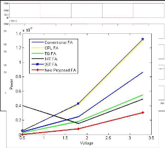
Simulation results are performed with PSPICE simulation software. The supply voltage ranges from 0.5V to 3.3V. The operating frequency is 5MHz for supply voltages above 1V, and 0.05MHz for supply voltages below 1V. The snapshot of the waveforms at 1.8V is shown in Figure 9.
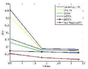
Plots of power versus voltage comparison are plotted in fig 10 and plots of delay versus voltage comparison are plotted in fig
11 considering new proposed fa. The excessive power and delay causes due to problem of the threshold voltage drop and the poor driving capability of some internal nodes at input
combinations that creates non-full swing transitions. The de- lay of the conventional adder decreases faster with the supply voltage comparing other adder cells. Simulation results also show that the new cell can work reliably at low supply voltag- es down to 0.5v at 0.05MHz comparing other adder cells. Fur- thermore, tga and 14t were made with less transistor number than others have, and additional buffers are required at each output to boost up its drivability, which increases their short circuit and switching power. However, it is observed that the new proposed full adder cell is the most energy efficient and faster operated cell compared with other design. Moreover this new design is made with less transistor number than oth- er adders.
The two main purpose of this work are power reduction and speed increase in the full adder circuit. In this operation, the GDI technique was introduced. By using techniques such as size, optimizing in full adder could reduce the power con- sumption. As a result, the full adder works at the 0.05 MHz speed with 0.0803 μw power consumption at 0.5V. On the oth- er hand, the lowest delay has been obtained at 3.3V which works at 5MHz speed and that is 0.01309 ns. The advantage of this new design is that this adder is not only energy efficient and faster but also it has less area with respect to transistor number. But the output voltage level of this design is not so good compared with other adders.
The authors wish to thank God and their Parents.
[1] Alireza Saberkari Shahriar Baradaran Shokouhi, ―A Novel Cmos 1-Bit Full Adder Cell With The Gdi Technique‖, College of Electrical Engineering, Iran University of Science & Technology, Tehran, Iran
[2] A. Morgenshtein, A. Fish, I. A. Wagner, ―Gate Diffusion Input (GDI) – A Novel Power Efficient Method for Digital Circuits: A Design Methodolo- gy,‖ 14th ASIC/SOC Conference, Washington D.C., USA, September
2001.
[3] Zimmermann, R. and W. Fichtner, 1997, ―Low-power logic styles: CMOS
versus pass-transistor logic‖, IEEE Journal of Solid-State Circuits, 32,
1079-1090.
[4] Issam, S., A. Khater, A. Bellaouar and M. I. Elmasry, 1996, ―Circuit tech- niques for CMOS lowpower high performance multipliers‖, IEEE Journal of Solid-State Circuits, 31, 1535-1546
[5] Zhuang, N. and H. Wu, 1992, ―A new design of the CMOS full adder‖,
IEEE Journal of Solid-State Circuits, 27, 840–844
[6] Weste, N. and K. Eshragian, 1993, ―Principles of CMOS VLSI Design: A System Perspective‖, PP: 531.
[7] Abu-Shama, E. and M. Bayoumi, 1996, ―A new cell for low power a d- ders‖, In: Proceedings of IEEE International Symposium on Circuits and Systems, Atlanta, GA, USA, pp. 49-52
IJSER © 2012
International Journal of Scientific & Engineering Research Volume 3, Issue 7, July-2012 5
ISSN 2229-5518
[8] Chang, C. H., M Zhang and J. Gu, 2003 of Conference, "A novel low power low voltage full adder cell" In: The 3rd International Symposium on Image and Signal Processing and Analysis (ISPA), pp. 454-458.
IJSER lb)2012
htt p://www .'lser. ora