International Journal of Scientific & Engineering Research, Volume 4, Issue 8, August 2013 1496
ISSN 2229-5518
A Lower-Power Pass Transistor Based Multiband
Flexible Divider with Integrated P & S Counter
Saima Mohammed Ali, Jobi Jose
Abstract—A lower-power single-phase clock multiband flexible divider with integrated P&S counter is presented. In order to enhance the working frequency of the counter, a modified form of extended true-single-phase-clock (E-TSPC) based divide-by-2/3 counter, which requires only one transistor to implement both the counting logic and the mode selection control, is used in the project. Here the gate count is reduced to a lower level by replacing the separate P –counter and S –counter used in the previous method by a single programmable integrated PS counter. This produces a multiband flexible divider with a lower power of about 11mW and a reduced gate count of about
225 and operates in 2.4 to 5 GHz and is applicable for Zigbee/IEEE 802.15.4.
Index Terms— DFF, dual modulus prescaler, dynamic logic, E-TSPC, frequency synthesizer, high-speed digital circuits, true single-phase clock (TSPC).
1 INTRODUCTION
—————————— ——————————
HE use of short range wireless communications created new protocols that define all parts of communication net- work including physical layer. The emerging of wireless sensor and telemetry network systems, such as ZigBee, de- mands for low-power low-cost wireless radio-frequency trans- ceivers, in order to achieve long operation time. Technical re- quirements, e.g. phase noise and channel spacing, for short- range, low data rate wireless communication systems are much relaxed. Therefore power dissipation is the most im- portant requirement. Frequency synthesizer is one of the most critical and power-hungry components in wireless transceiver.
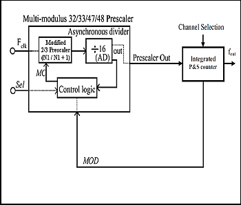
Fig. 1. Multiband flexible divider using integrated p&s counter.
————————————————
• Saima Mohammed Ali is currently pursuing master’s degree program in ap- plied electronics engineering in Mahatma Gandhi University, India. E-mail: saimamohdali3@gmail.com
• Jobi Jose is currently working as an assistant professor in ICET, Kerala, India. E-mail: jobibose03@yahoo.com
The rapid evolution of the communications industry has greatly increased the demand for lower cost, lower power and wider bandwidth RF circuits operating at microwave frequen- cies with higher level of integration. In the previous design [1], a dyamic logic multiband flexible integer-N divider based on pulse-swallow topology is proposed which uses a low-power wideband 2/3 prescaler [10] and a wideband multimodu- lus32/33/47/48.
In this paper a new method for designing a dynamic logic multiband flexible integer-N-divider has been proposed which was developed using a wideband multimodulus 32/33/47/48 prescaler with a pass transistor based low-power wideband
2/3 prescaler and an integrated P & S counter as shown in Fig.
1. Swallow counter (S-counter) which was used in design [1]
has been replaced by a simple digital circuit.
2 DESIGN CONSIDERATIONS
In the case of high-speed digital circuits propagation delay and power consumption are the important parameters. The maximum operating frequency of a digital circuit is given by,
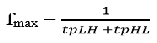 (1) The tpLH and tpHL denote the propagation delays of the low-
to-high and high-to-low transitions of the gates, respectively.
The CMOS digital circuits total power consumption is deter-
mined by the switching and short circuit power. The switch-
ing power is linearly proportional to the operating frequency
and is given by the sum of switching power at each output
node as in
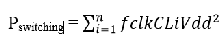
(2)
IJSER © 2013 http://www.ijser.org
International Journal of Scientific & Engineering Research, Volume 4, Issue 8, August 2013 1497
ISSN 2229-5518
Where n is the number of switching nodes, fclk is the clock fre- quency, CLi is the load capacitance at the output node of the ith stage, and Vdd is the supply voltage. Normally, the short-circuit power occurs in dynamic circuits when there exists direct
paths from the supply to ground which is given by
Psc = Isc * Vdd (3) Where Isc is the short-circuit current. The short-circuit power is
much higher in E-TSPC logic circuits than in TSPC logic cir-
cuits. However, TSPC logic circuits exhibit higher switching
power compared to that of E-TSPC logic circuits due to high
load capacitance. For the E-TSPC logic circuit, the short-circuit
power is the major problem. The E-TSPC circuit has the merit
of higher operating frequency than that of the TSPC circuit due to the reduction in load capacitance, but it consumes sig- nificantly more power than the TSPC circuit does for a given transistor size. The following analysis is based on the latest
design using the popular and low-cost 0.18-μmCMOS process.
3 DIVIDE BY 2/3 COUNTER DESIGN
The two FFs and the NOR gate are used in design [2]. The log- ic structure of the proposed design is shown in Fig. 2. The NOR gate is equivalent to bubbled AND gate. The NOR gate for the divide control (mode control) is replaced with a switch.
the divide control signal serves as the switch. The AND gate plus its input inverter are achieved by way of wired-AND logic using no extra transistors at all. The proposed design scheme is far more sophisticated than the measure of simply adding one pass transistor may suggest. First of all, unlike any previous designs, the E-TSPC FF design remains intact with- out any logic embedding. Both speed and power behaviors are not affected, which indicates a performance edge over the log- ic embedded FF design. Secondly, the inverter to complement the one of the two E-TSPC FF outputs for divide-by-3 opera- tions is removed in the proposed design. The circuit simplifi- cation, again, suggests the improvements in both speed and power performances. The working principle of the proposed design is elaborated as follows. When DC is “1”, the pMOS transistor PDC is turned off as a switch should behave. A single pMOS transistor, however, presents a smaller capacitive load to FF1 than an inverter does in design [7]. When DC is “0”, the output of FF1, Q1b, is tied with the output node of the 1st stage inverter of FF2 through the pMOS transistor. In an E- TSPC FF design, the output of the first stage inverter can be regarded complementary to the input D, i.e., . Therefore, a wired-OR logic is in fact implemented. Either Q2b being “0” or Q1b being “1” pulls the output node of the inverter high. This means D2b = Q1b +
 . By applying Demorgan’s law to the to the Boolean equation gives rise to
 = D2 =
  , which is exactly the desired logic. Since Q1b is applied to the input of
  , theinverter needed to complement the Q1b signal can be eliminated.
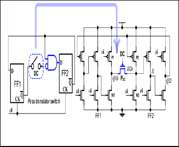
Fig. 2. E-TSPC-based Logic structures of divide-by-2/3 counter de- sign.
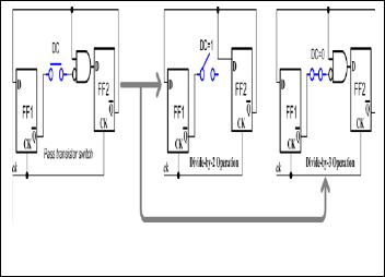
Note that there is a negation bubble at one of the AND gate’s input. The output of FF1 is thus complemented before being fed to FF2. When the switch is open, the input from FF1 is disconnected and FF2 alone divides the clock frequency by
2. When the switch is close, similar to the design in [7], FF1 and FF2 are linked to form a counter with three distinct states. Fig. 3 shows the circuit implementation. According to the simulation results given in [12], E-TSPC design shows the best speed performance in various counter designs including the one using conventional transmission gate FFs. Besides the speedadvantage, E-TSPC FFs are particularly useful for low voltage operations because of the minimum height in transis- tor stacking. Other than the two E-TSPC FFs, only one pMOS transistor (PDC ) is needed. The PMOS transistor controlled by
Fig. 3. MOS schematics of divide-by-2/3 counter design with pass transistor logic circuit technique.
4 MULTIMODULUS 32//33/47/48 PRESCALER
The proposed wideband multimodulus prescaler is similar to the 32/33 prescaler, but with an additional inverter and a mul- tiplexer. The proposed prescaler can divide the input frequen- cy by 32, 33, 47, and 48 is shown in Fig. 4. It performs addi- tional divisions (divide-by-47 and divide-by-48) without any extra flip-flop, thus saving a considerable amount of power and also reducing the complexity of multiband divider.
The multimodulus prescaler consists of the wideband 2/3
IJSER © 2013 http://www.ijser.org
International Journal of Scientific & Engineering Research, Volume 4, Issue 8, August 2013 1498
ISSN 2229-5518
(N1 / (N1 + 1)) prescaler, four aysnchronous TSPC divide-by-2 circuits ((AD) = 16) and combinational logic circuits to achieve multiple division ratios. Besides the usual MOD signal for controlling N / (N + 1) divisions, the additional control signal Sel is used to switch the prescaler between 32/33and 47/48 modes.
A. Case 1: Sel = 0
When Sel = 0, the output from the NAND2 gate is directly
transferred to the input of 2/3 prescaler and the multimodulus
prescaler operates as the normal 32/33 prescaler, where the
division ratio is controlled by the logic signal MOD. If MC = 1,
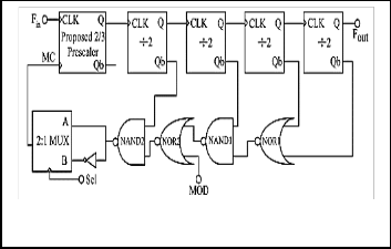
the 2/3 prescaler operates in the divide-by-2 mode and when
Fig. 4. 32/33/47/48 multimodulus type prescaler.
MC = 0, the 2/3 prescaler operates in the divide-by-3 mode. If
MOD = 1, the NAND2 gate output switches to logic “1” (MC =
1) and the wideband prescaler operates in the divide-by-2
mode for entire operation. The division ratio N performed by
the multimodulus prescaler is
N = (AD * N1 ) + (0 * (N1 + 1)) = 32 (4) Where N1 = 2 and AD = 16 is fixed for the entire design. If
MOD = 0, for 30 input clock cycles MC remains at logic “1”,
where wideband prescaler operates in divide-by-2 mode and, for three input clock cycles, MC remains at logic “0” where the wideband prescaler operates in the divide-by-3 mode. The division ratio N + 1 performed by the multimodulus prescaler
is
N + 1 = ((AD – 1) * N1 ) + (1 * (N1 + 1)) = 33 (5)
B. Case 2: Sel = 1
When Sel = 1, the inverted output of the NAND2 gate is di- rectly transfered to the input of 2/3 prescaler and the multi- modulus prescaler operates as a 47/48 prescaler, where the division ratio is controlled by the logic signal . If MC = 1, the
2/3 prescaler operates individe-by-3 mode and when MC = 0, the 2/3 prescaler operates individe-by-2 mode which is quite opposite to the operation performed when Sel = 0. If MOD = 1, the division ratio N + 1 performed by the multimodulus pre- scaler is same as (4) except that the wideband prescaler oper- ates in the divide-by-3 mode for the entire operation given by
N + 1 = (AD * (N1 + 1)) + (0 * N1 ) = 48 (6)
If MOD = 1, the division ratio N performed by the multi- modulus prescaler is
N = ((AD – 1) * (N1 + 1)) + (1 * N1 ) = 47 (7)
5 INTEGRATED P AND S COUNTER
Fig. 5 shows the block diagram of Integrated P&S counter. As it is apparent, this counter consists of a divide-by-64 (P counter) that is made up of 6 divide-by-2. Digital circuit con- sists of XNOR gates (X0 – X4), AND gates (A1, A2) and a RE- SETSET Flip Flop (RSFF). This digital section has replaced S counter in conventional ones and has the duty to control modulus bit of dual modulus prescaler. A1 gate is driven by XNOR gates (X0 – X4). Table I shows the output of XNOR block for 4 available inputs. As it’s clear, XNOR gate is an equality block. When inputs of XNOR are equal (both of them are 0 or 1), output of XNOR gate is logic one. So when the val- ue of P counter (P5P4P3P2P1P0) is equal to predefined C number (1C4C3C2C1C0), output of A1 gate becomes logic 1 (C4- C0 bits are defined by transceiver system that changes the frequency channel of PLL). In this moment, as P5 is 1 as well, RSFF is set by A2 gate and dual modulus prescaler divide in- put frequency by N. When P5 changes to 0, RSFF is reset and dual modulus prescaler return to divide-by-(N + 1) state. For more details, assume the P counter is in ZERO condition
{P5P4P3P2P1P0=000000}. As P5 is equal to 0, RSFF is reset and dual modulus prescaler divides input frequency by (N + 1). Inorder for the PLL to work in 6th frequency channel and we load the number of 6 on C4-C0 {C4C3C2C1C0=00110}. Input signal is applied and P counter increases until the value of P counter reaches the predefined C {P5P4P3P2P1P0 =
1C4C3C2C1C0} (For this example: P5P4P3P2P1P0 = 100110). In this value of P counter, output of XNOR blocks and P5 are logic 1 that causes RSFF to be set by A1 and A2 gates. After this time, the prescaler divide input frequency by N till the P counter reaches to its maximum value (111111) and next value is 000000. RSFF is reset by P5, prescaler returns to divide-by- (N + 1) situation and the cycle repeats again. In this cycle the events occurred similar to conventional pulse Swallow divid- er. For the quantity of predefined C (1C4C3C2C1C0=C), pre- scaler divide input frequency by (N + 1) and for rest of num- ber (64 – C) it divides input frequency by N. For a cycle we will have:
A. Case 1: Sel =0
The frequency division (FD) ratio of the multiband divider in this mode is given by:
FD = (N + 1) * S + N * (P – S) = NP +S (8) Substituting P = 64, S = C in the above equation, we get:
FD = N * 64 + C (9)
IJSER © 2013 http://www.ijser.org
International Journal of Scientific & Engineering Research, Volume 4, Issue 8, August 2013 1499
ISSN 2229-5518
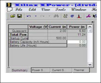
TABLE 1
TRUTH TABLE OF XNOR GATE
Input 1 | Input 2 | Output |
0 | 0 | 1 |
0 | 1 | 0 |
1 | 0 | 0 |
1 | 1 | 1 |
B. Case 2: Sel =1
The frequency division (FD) ratio of the multiband divider in this mode is given by:
FD = (N * S) + (N + 1) * (P – S) = (N + 1) P – S (10) Substituting P = 64, S = C in the above equation, we get:
FD = (N + 1)* 64 – C (11)
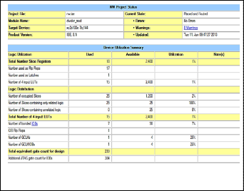
Fig. 6. Power consumption obtained using Xilinx.
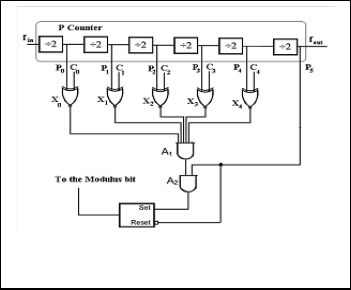
Fig. 7. Gate count obtained from Xilinx simulation.
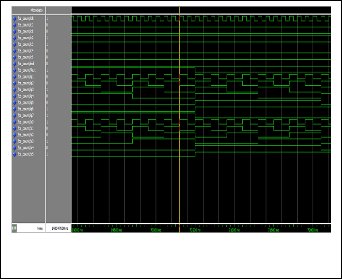
Fig. 5. Integrated P&S counter (6 bit P-counter and 5 bit programma- ble S-counter).
6 SIMULATION RESULTS
The simulation of the design is performed using Xilinix and Modelsim. The proposed multiband flexible divider consumes power of 11 mw and has a gate count of 225. The power con- sumption, gate count and area of the previous programmable dividers and the proposed programmable divider at the sup- ply voltage of 1.8V is shown in Table II
Fig. 8. Simulation waveforms of integrated P&S counter.
IJSER © 2013 http://www.ijser.org
International Journal of Scientific & Engineering Research, Volume 4, Issue 8, August 2013 1500
ISSN 2229-5518
TABLE 2
COMPARISON OF PRESENT METHOD W ITH OLD METHOD
| Old System [1] | Proposed System |
Power | 29 mw | 11 mw |
Gate Count | 636 | 225 |
Area | Large | Small |
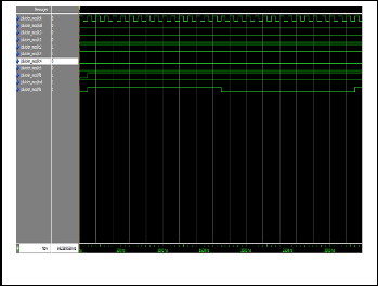
Fig. 9. Simulation waveform of divider (Sel = 0; Mod = 1).
7 CONCLUSION
In this paper a lower-power single-phase clock multiband flex- ible divider with integrated P&S counter is presented. The Swallow counter which consumes a large portion of energy in conventional frequency divider is replaced by a simple digital section in this structure. Also the pass transistor based divide- by-2/3 counter successfully simplifies the control logic and one pMOS transistor alone serves the purposes of both mode select and counter excitation logic. In the paper, the circuit simplicity leads to reduced power consumption, reduced number of gates required and hence a reduced area require- ment.
REFERENCES
[1] Vamshi Krishna Manthena, Manh Anh Do, Chirn Chye Boon, and Kiat Seng Yeo., “A Low-Power Single-Phase Clock Multiband Flexi- ble Divider” , IEEE Trans. Very Large Scale Integr, (VLSI) Syst., vol. 20, no. 2, Feb. 2012
[2] Yin-Tsung Hwang and Jin-Fa Lin., “Low Voltage and Low Power Divide-By-2/3 Counter Design Using Pass Transistor Logic Circuit Technique”, IEEE Trans. Very Large Scale Integr.(VLSI) Syst., vol. 20, no. 9, Sep. 2012
[3] Ali Sahafi, Jafar Sobhi, Mahdi Sahafi, and Omid Farhanieh, “An Ul-
tra-Low Power Frequency Divider for 2.4GHz Zigbee Frequency Synthesizer”, ELECO 2011 7th International Conference on Electrical and Electronics Engineering, 1-4 December, Bursa, TURKEY
[4] A.J. Gines, A.Villegas, A.J. Acosta, M.A. Jalon, D.Vazquez, A.Rueda and E.Peralias, “A 1.2V .14mW Quadrature Frequency Synthesizer in
90nm CMOS Technology for 2.4GHz Zigbee Applications”, IEEE APPCAS, pp. 1252-1255,Nov. 2008.
[5] Roberto Nonis, Enzo Palumbo, Pierpaolo Palestri and Luca Selmi, “A Design Methodology for MOS Current-Mode Logic Frequency Di- viders”, IEEE Trans. Circuits & Systems-I: Reg. Papers, vol. 54, no.2, pp.
245-254, Feb. 2007.
[6] S. Pellerano et al., “A 13.5-mW 5 GHz frequency synthesizer with dynamic-logic frequency divider,” IEEE J. Solid-State Circuits, vol. 39, no. 2, pp. 378–383, Feb. 2004.
[7] S. Pellerano, S. Levantino, C. Samori, and A. L. Lacaita, “A 13.5-mW
5-GHz frequency synthesizer with dynamic-logic frequency divider,”
IEEE J. Solid-State Circuits, vol. 39, no. 2, pp. 378–383, Feb. 2004.
[8] S. Shin et al., “4.2 mW frequency synthesizer for 2.4 GHz ZigBee application with fast settling time performance,” in IEEE MTT-S Int. Microw. Symp. Dig. , Jun. 2006, pp. 411–414.
[9] S. Vikas et al., “1 V 7-mW dual-band fast-locked frequency synthe- sizer,” in Proc. 15th ACM Symp. VLSI, 2005, pp. 431–435.
[10] V. K. Manthena et al., “A 1.8-V 6.5-GHz low power wide band single phase clock CMOS 2/3 prescaler,” in IEEE 53rd Midwest Symp. Cir- cuits Syst., Aug. 2010, pp. 149–152.
[11] J. M. Rabaey et al., “Digital integrated circuits, a design perspective,”
in Ser. Electron and VLSI, 2nd ed. Upper Saddle River, NJ: Prentice- Hall, 2003.
[12] Y.-L. Lo, T.-S. Chao, and K.-H. Cheng, “High speed and ultra-low voltage divide-by-4/5 counter for frequency synthesizer,” IEICE Trans. Electron., vol. E92-C, no. 6, pp. 890–893, Jun. 2009.
[13] Yu, X.P., et al, “Design of a low power wide-band high resolution programmable frequency divider,” IEEE trans. VLSI, Vol.13, No.9, pp.1098-1103, Sep., 2005.
[14] M. Alioto and G. Palumbo, “Model and Design of Bipolar and MOS Current-Mode Logic Digital Circuits”. New York: Springer, 2005.
[15] M. Vamshi Krishna, et.al, “A low power fully programmable 1MHz resolution 2.4GHz CMOS PLL frequency synthesizer”, in Proc. IEEE Biomedical Circuits & Systems Conf., pp. 187-190, Nov 2007.
[16] G. C. T. Leung and H. C. Luong, “A 1-V 5.2-GHz CMOS synthesizer for WLAN applications,” IEEE J. Solid-State Circuits, vol. 39, no. 11, pp. 1873–1882, Nov. 2004.
[17] Z. Deng and A. M. Niknejad, “The speed-power trade-off in the de- sign of CMOS true-single-phase-clock dividers,” IEEE J. Solid-State Circuits, vol. 45, no. 11, pp. 2457–2465, Nov. 2010.
[18] Ting-Hsu Chien, Chi-Sheng Lin, “High Speed and Low Power Pro- grammable Frequency Divider” in IEEE International Symposium on Circuits and Systems (ISCAS), Paris, France, 2010, pp. 4301-4304.
[19] Zhiqiang, Gao, Yuanxu Xu, “A Programmable High-Speed Pulse Swallow Divide-by-N Frequency Divider for PLL Frequency Synthe- sizer” in International Conference on Computer Application and System Modeling (ICCASM), 2010, pp. V6-315 - V6-318
[20] J. N. Soares, Jr and W. A. M. Van Noije, “Extended TSPC structures with double input/output data throughput for gigahertz CMOS cir- cuit design,” IEEE Trans. Very Large Scale Integr. (VLSI) Syst., vol. 10, no.3, pp. 301–308, Jan. 2002.
[21] S. Pellerano, S. Levantino, C. Samori, and A. L. Lacaita, “A 13.5-mW
5-GHz frequency synthesizer with dynamic-logic frequency divider,”
IJSER © 2013 http://www.ijser.org
International Journal of Scientific & Engineering Research, Volume 4, Issue 8, August 2013 1501
ISSN 2229-5518
IEEE J. Solid-State Circuits, vol. 39, no. 2, pp. 378–383, Feb. 2004.
[22] X.-P. Yu, M. A. Do, W. M. Lim, K. S. Yeo, and J. G. Ma, “Design and optimization of the extended true single-phase clock-based pre- scaler,”IEEE Trans. Microw. Theory Techn, vol. 54, no. 11, pp. 3828–
3835,
Nov. 2006.
[23] R. S. Rana, “Dual-modulus 127/128 FOM enhanced prescaler design in 0.35 um CMOS technology,” IEEE J. Solid-State Circuits, vol. 40, no.
8, pp. 1662–1670, Aug. 2005.
[24] Z. Deng and A. M. Niknejad, “The speed-power trade-off in the de- sign of CMOS true-single-phase-clock dividers,” IEEE J. Solid-State Circuits, vol. 45, no. 11, pp. 2457–2465, Nov. 2010.
[25] M. V. Krishna, M. A. Do, K. S. Yeo, C. C. Boon, and W. M. Lim, “De- sign and analysis of ultra low power true single phase clock CMOS
2/3 prescaler,” IEEE Trans. Circuits Syst. I, Reg. Papers, vol. 57, no. 1, pp. 72–82, Jan. 2010.
[26] Y.-L. Lo, T.-S. Chao, and K.-H. Cheng, “High speed and ultra low voltage divide-by-4/5 counter for frequency synthesizer,” IEICE
Trans. Electron., vol. E92-C, no. 6, pp. 890–893, Jun. 2009.
IJSER © 2013 http://www.ijser.org