q
distance (wcr) and desired value of capacitance. Each of these quantities can be expressed in term of the structural parame-
Δ Δ w (x ,y ) =
D
International Journal of Scientific & Engineering Research Volume 4, Issue 2, February-2013 1
ISSN 2229-5518
A Generalized model for the design of MEMS
electrostatic actuators
Anurekha Sharma
Abstract— The MEMS sensing and actuating devices make use of the electrostatic principle. A number of MEMS structures make use of deformation and/or pull in of the diaphragms and beams for performing sensing and actuation. The electrostatic actuator may have air as a dielectric or may have an intervening layer of dielectric or multilayered dielectric along with air-gap. For any of these structures the design specification is given in terms of the pull-in Voltage (VPull) and desired value of capacitance. The paper presents a semi-analytical technique for determining the generalized expression for pull-in voltage, critical distance and capacitance at pull-in for all the three types of structures. It has been found that for an actuator with only a single intervening layer of dielectric, the dielectric constant greater than 10 is not desirable, thus SiO2, Si3N4 are the only choices. However, if multilayer structure is used, high K materials can be used. For given
structural parameters and material properties, it has been found that a figure of merit can be given as V 2 C3
=9.94×10⁻²⁰ Da 2 , a is the half
side length of the square diaphragm, D is flexural rigidity .Using these equations one can find the pull-in voltage as well as predict the capacitance for the actuator, for the given structural and material properties. One can also decide the thickness of the dielectric for a given air-gap to achieve a specified value of pull-in.
—————————— ——————————
The MEMS sensing and actuating devices make use of the electrostatic principle. A number of MEMS structures make use of deformation and/or pull in of the diaphragms and beams for performing sensing and actuation. The diaphragms may be circular, square or rectangular. Square diaphragms find use in numerous applications like electrostatic valve actu- ator for high-pressure applications [1], polysilicon micro- mirrors [2], silicon capacitive microphone [3], micropumps [4], bio-medical applications [5] as well as in touch-mode pressure sensors [6]. When these devices are used as actuators, the criti- cal design parameters are pull-in voltage (VPull) [7], critical
The typical structure of the electrostatic transducer with a single layer of dielectric is as shown in Fig. 1. According to the classic theory of plate bending, a small-deflection case is de- fined as a case where the displacement of the middle plane is small compared to the plate thickness [6]. The relation be- tween the lateral load q and the deflection w(x,y) at any point (x,y) of a plate in the case of small deflection is given by :
q
distance (wcr) and desired value of capacitance. Each of these quantities can be expressed in term of the structural parame-![]()
Δ Δ w (x ,y ) =
D
(1)
2 2
ters and material properties of the diaphragm. It is well known that for an actuator with air gap, pull-in occurs at a
where w is deflection of the plate mid-surface , Δ =
![]()
x 2
,
y 2
critical displacement equal to one-third of the gap between the electrodes[7]. Employing an intervening layer of dielectric or multilayered layered dielectric on the fixed electrode can in- crease the pull-in voltage and critical distance. The ratio of thickness of the dielectric medium to its dielectric constant denoted by deff determines the pull-in voltage and capaci- tance. The paper presents a semi-analytical technique for de- termining a generalized expression of pull-in voltage, critical distance and capacitance at pull-in for an electrostatic actuator
q is the normal load per unit area, D is flexural rigidity=
E h 3 / 1 2 (1 -υ 2 )
, E is Young’s modulus of the diaphragm ma-
terial, h is the thickness of the diaphragm and ? is the Pois- son’s ratio.
In the presence of applied pressure and applied voltage, (1)
is modified as :
P + P
with only air as a dielectric or along with a single layer of die- lectric or multilayered dielectric for a square diaphragm
————————————————
![]()
Δ Δ w = e l (2)
D
where, Pel is the electrostatic pressure and P is the mechan- ical pressure. The electrostatic pressure Pel is given as :
Pe l =
![]()
ε 0 ε r V 2
2 d 2
(3)
where, d is distance between the plates, is relative per-
mittivity of the medium or the dielectric constant of the medi-
um and is permittivity of free space.
IJSER © 2013 http://www.ijser.org
International Journal of Scientific & Engineering Research Volume 4, Issue 2, February-2013 2
ISSN 2229-5518
rewritten in a generalized form as :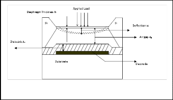
V2
DΔΔw P+ε0
2(d
eff
+(d0
w))2
![]()
(7)
where deff = tm/i (for a single layer of dielectric) and deff
= d1/1 + d2/2 (in case of a layered dielectric), in general
deff = d1/1 + d2/2 + -------------+ dn/n (for a n-layered die- lectric)
Fig 1. Cross-sectional view of electrostatic transducer with a single layer of dielectric
The diaphragm deflection w(x, y) with air as dielectric is given by considering that the distance d between the plates changes to due to the displacement w of the diaphragm in the presence applied pressure and voltage as shown in figure 1. Therefore, substituting (3) in (2) for air gap , the equation be- comes :
2
V
![]()
DΔΔw P+ε0εa 2
2(d0 w)
For diaphragm with intervening layer of dielectric
2
(4)
Fig 3. Co-ordinate system and dimensions for a square diaphragm
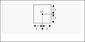
The boundary conditions for the square diaphragm with clamped edges are as follows
The deflection w(x, y) = 0 at x = , y = , = 0, = 0 at x =, y =,
DΔΔw P ε2ε ε
V
![]()
2(εa tm +εid0 w))
(5)
x = 0 and at y = 0
where 2a is the side length of the diaphragm ( fig. 2)The
approximate solution that satisfies the above given boundary
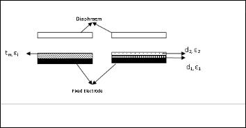
For a layered dielectric with two dielectric layers of thick- ness d1 and d2 with dielectric constants ε1 andε2 respectively
conditions is :
2 2 2 2 2 2
(Fig. 2) , the equation becomes :![]()
D ΔΔw P ε ε 2 ε 2 ε V
a 1 2 0 2(ε ε d +ε ε d +ε ε (d
(6)
w )) 2
w (x ,y ) = λ (x -a ) (y -a ) (8)
where λ is a function which depends on voltage V, dia- phragm thickness h , Young’s modulus E , Poisson’s ratio υ
where d0 is zero pressure gap, is the dielectric constant of the air, is the dielectric constant of the insulator,is permittivity of free space = 8.85x10⁻¹² F/m and is the thickness of the insu-
and dielectric constant εr of the medium. The equation govern- ing λ for air as dielectric is calculated by substituting eq. (8) in eq. (7) and is given by [8] :
lator.![]()
λ3 +λ2 ( 2d0
![]()
49P
2d
![]()
eff )+
a8 2304a4D a8
d2 49d P 2d d 49 Pd d2
λ( 0 + 0 + 0 eff +
![]()
eff
![]()
+ eff )
(9)
a16
1152a12 D a16
2
1152a12ε D a16
2 2
![]()
( 49d0 P
![]()
+ 49d0deff P
![]()
+ 49Pdeff
![]()
49ε0 V
) 0
2304a20D 1152a 20 D 2304a 20D 4608a 20D
Fig 2. Representation of single and multi-layered dielectric on a fixed electrode
As εa =1, Eq. (5), Eq. (6) and Eq.(7) can be combined and
For determining the pull-in voltage the real root of λ in (9) is evaluated at x=0 and y=0. The resulting expression for de- flection is differentiated with respect to voltage and solved for pull-in voltage by equating to zero. The critical distance is got by substituting the pull-in voltage for voltage V in expression for deflection.
For air as dielectric the expression for the pull-in voltage
(Vpull) and critical distance (wcr) is given as:
IJSER © 2013 http://www.ijser.org
International Journal of Scientific & Engineering Research Volume 4, Issue 2, February-2013 3
ISSN 2229-5518
Vpull =![]()
3 2 2 (d 0 +d eff ) D
7 a 3 ε
(10)
C0=
ε0 A
![]()
deff + d0
wcr =
0
d d
![]()
![]()
0 + e ff
3 3
(11)
The Capacitance is given as :
+a +a
C=
![]()
ε 0 dxdy
(12)
-a -a deff +(d0 -w)
The above relations have been verified by simulation with Intellisuite and the results are in agreement with the simulated ones [8]. At Pull-in
(a)
32 2 (3wcr ) D

Vpull =
7a2 3 ε
ε A
(13)
Cpull ~ 0 A is the area of cross-section of the
w
![]()
d +(d - cr )
eff 0 3
diaphragm
The figure of merit is given by
V 2 C 3 = 9.9 4×10 -20 D a 2 m3 (14)
Eq. (14) along with (10), (11) and (12) can be used to design a transducer for a given pull-in voltage or capacitance.
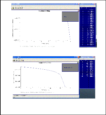
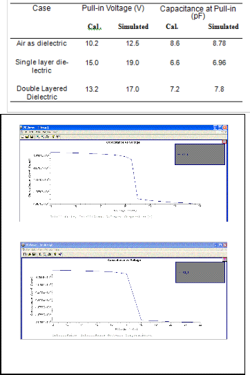
Table I gives the comparison between the simulated and calculated values of pull-in voltage and capacitance for a sili- con diaphragm (E=130 GPa) of half side length a=661µm, thickness h=5.1µm, air-gap d0=2µm
TABLE 1.
COMPARISON BETW EEN THE CALCULATED AND SIMULATED PARAME- TERS FOR AIR AS DIELECTRIC
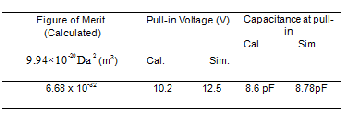
Figure 4a and 4b shows the simulated results for the above case.
A. Effect of layered –dielectric on the pull-in voltage and
Capacitance of electrostatic transducer
The zero-voltage capacitance is given as
(b)
Fig 4. (a) Pull-in Voltage from displacement versus voltage (b) Capaci- tance versus voltage
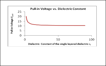
From (10) it can be seen that the pull-in voltage varies as (deff) 1.5 whereas capacitance varies inversely as deff. So, as the dielectric constant of the medium increases for a given thick- ness of dielectric Vpull decreases more rapidly as compared to increase in capacitance. The fig. 5 shows that Vpull saturates for values of dielectric constant >10, so the obvious choice of die- lectric when a single layer of dielectric is used is SiO2 or Si3N4. However, if one wants to have more flexibility in design then the layered dielectric is a good proposition.
Fig 5. Effect of the dielectric constant on the pull-in voltage (diaphragm dimensions a=661 µm, h= 5.1 µm ,tm=2.3 µm E= 130 GPa, d0=2.0 µm)
IJSER © 2013 http://www.ijser.org
International Journal of Scientific & Engineering Research Volume 4, Issue 2, February-2013 4
ISSN 2229-5518
Let us now define the normalized pull-in voltage and normalized capacitance in the following manner![]()
t m >
εi
![]()
![]()
d1 d2
εi ε2
3 2 2
( d + d ) 3 D
Now, let us consider that = ptm (where 0<p<1) , therefore
Vnor =
V p u ll-d i e
![]()
=
7 a 2
3 ε 0
, where Vpull-air is
d2 = (1-p)tm also let 2= Ki where K is any number greater than zero. The above equation becomes
V p u ll-a i r
3 2 2 d 0 D![]()
![]()
![]()
m > pt m (1-p)t m
=> 1 >
![]()
p (1-p)
7 a 2
3 ε 0
εi εi Kεi K

the pull-in voltage for air as dielectric and Vpull-die is the pull-in voltage with an intervening layer of dielectric or layered die- lectric .
3 / 2
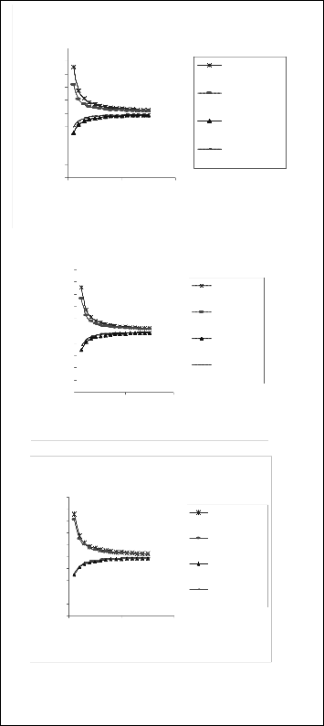
For the above inequality to be satisfied, K>1. The fig 6. shows the variation of normailsed pull-in voltage and normal- ized capacitance for a single layer of dielectric and a layered dielectric for d0 = 2.0µm, tm=2.3 µm for different values of i
Vnor = 1+
deff
![]()
(15)
starting from 2. The graphs clearly indicate that significant
d0
increase in capacitance can be brought about if the layer with
lower dielectric constant is thinner
For a single layer of dielectric :
3/2
t
Case II 1=K1 i and 2= K21 , then if Cnor2 > Cnor1 we have
Vnorsingle = 1+ m
(16)
ε i d0
1 (1-p) ![]()
![]()
1 > p
and for a layered dielectric with two dielectric materials normalized pull-in voltage is :
K1
K2
d d
3/2
K2 1, as it would mean single layer of dielectric, thus the![]()
Vnordouble = 1+ 1![]()
2
(17)
above inequality would be satisfied for K1 >1 and K2 >1. K2
ε1d0
ε2 d0
=K1 is also admissible.
The capacitance is normalized with respect to capacitance with air-gap and is given as :![]()
ε 0 A
The fig. 7 shows the variation of normalized capacitance
as well as pull-in voltage for the single layer as well as double
layer. Table II compares the pull-in voltage for air, single lay-
ered dielectric and double layered dielectric and Figures 8a
Cnor =![]()
C d ie
![]()
![]()
d 0 + d e ff 1
and 8b give the simulated results of the capacitance for single
layered dielectric SiO2 (i =3.9) and multilayered dielectric
C a i r
ε 0 A![]()
d 0
d e ff![]()
1 +
d 0
consisting of lower layer of SiO2
Si3N4 ( 2
(1
=3.9) and upper layer of
2
For single dielectric, normalized capacitance is :
1
![]()
Cnorsingle =
(18)
=7.5) and p=.25 i.e. thickness of SiO
that of Si3N4 is 1.725µm.
.
is 0.575µm and
Cnordouble =![]()
1+ t m
εi d0
1
![]()
![]()
1+ d1
ε1d0
d2
![]()
ε 2 d0
(19)
Following conclusions have been drawn on the basis of the above discussion.
1. Design of the electrostatic transducer presents a trade- off between pull-in voltage and achievable capacitance. With the increase in the dielectric constant of the single layer, the
For attaining higher value of capacitance with a layered di-
electric with same overall thickness as the single layer i.e. d1+d2= tm requires Cnordouble > Cnorsingle
Therefore :
pull-in voltage decreases more rapidly as compared to in- crease in capacitance.
2. The maximum value of zero-gap capacitance in pres- ence of single as well multilayered dielectric is limited by the![]()
![]()
![]()
tm > d1 d 2
(20)
air gap. Similarly, the minimum value of the pull-in in both
εi ε1 ε2
Let 2 > 1, then the following cases arise
Case I When the lower layer is of the same material as the single layer dielectric, then 1= i , then Eq. (20) becomes
cases is limited by the air-gap.
3. The capacitance can be increased marginally if instead
of employing a single layer, one employs a double layer
4. A figure of merit is found, which can be used to design
electrostatic transducer for a given pull-in voltage irrespective
of the single, multi or no dielectric. This figure of merit serves
as a useful tool to find the geometric dimensions of the device.
IJSER © 2013 http://www.ijser.org
International Journal of Scientific & Engineering Research Volume 4, Issue 2, February-2013 5
ISSN 2229-5518
Using these equations one can find the pull-in voltage as well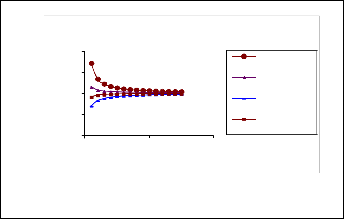
thickness of the dielectric for a given air-gap to achieve a par- ticular value of pull-in.
2
1.8
1.6
1.4
1.2
1
0.8
0.6
0.4
0.2
0
p=0.25
Single layer pull-in
Double-layer pull-in
Single layer
Capacitance
Double layer
Capacitance
2
1.5
1
0.5
0
0 20 40
Epsilon
Single layer pull-in Double layer pull-in
Single layer Capacitance Double layer capacitance
0 20 40
Eps ilon
p=0.5
Fig 7. Variation of Normalised capacitance and pull-in voltage
TABLE 2.
2
1.8
1.6
1.4
1.2
1
0.8
0.6
0.4
0.2
0
single layer pull-in
Double layer pull-in
Single layer capacitance
Double layer capacitance
COMPARISON OF PULL-IN VOLTAGE AND CAPACITANCE
0 20 40
Eps ilon
p=0.75
2
1.8
1.6
1.4
1.2
1
0.8
0.6
0.4
0.2
0
0 20 40
epsilon
Single layer pull- in
Double layer pull- in
Single layer
Capacitance
Double layer capacitance
(a)
Fig 6. Normalised Pull-in Voltage and Pull-in Capacitance for different thickness of lower layer of dielectric (a) 0.25 times the single layer (b) 0.5 times the single layer (c) 0.75 times the single layer
as predict the capacitance for the actuator, for the given structural and material properties. One can also decide the
(b)
Fig 8. Simulated Capacitance vs. Voltage for (a) single layered dielec- tric (b) for a double layered dielectric
IJSER © 2013 http://www.ijser.org
International Journal of Scientific & Engineering Research Volume 4, Issue 2, February-2013 6
ISSN 2229-5518
[3] Quanbo Zou,Zhimin tan, et. al., A novel integrated Silicon Capacitive- Floating electrode “Electret” Microphone (FEEM), Journal of Microelectro- mechanical Systems, Vol 7, No.2, pp. 224-234,1998.
[4] Eiji Makino, Takashi Mitsuya, Takayuki Shibata, Fabrication of TiNi
shape memory micropump, Sensors and Actuators , A88, pp256-262,2001.
[5] T. Goettsche , J. Kohnle , M. Willmann , H. Ernst , S. Spieth , R. Tisch-
ler ,S. Messner , R. Zengerle , H. Sandmaier, Novel approaches to particle
tolerant valves for use in drug delivery systems, Sensors and Actuators, A
118,pp. 70-77,2005.
[6] Qiang Wang, Wen H. Ko, Modeling of touch mode capacitive sensors and diaphragms, Sensors and Actuators, A 75,pp. 231- 241,1999.
[7] S.D Senturia, Microsystem Design (Boston, MA: Kluwer Academic, 2001) [8] Anurekha Sharma and P.J. George, A simple method for calculation of the pull-in voltage and touch-point pressure for the small deflection of square diaphragm in MEMS, Sensors and Actuators , A 141,pp.376-382,
2008.
(a)
(b)
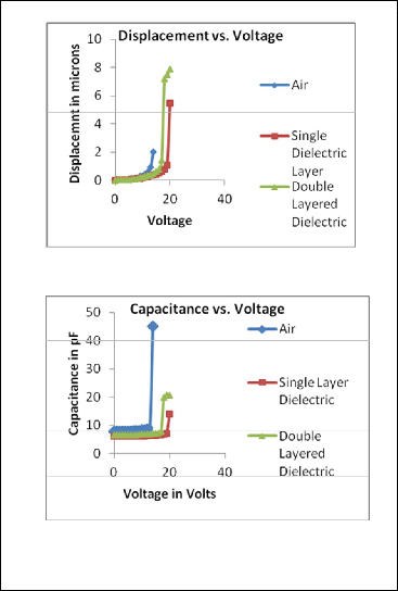
Fig. 9 Comparison of (a) Displacement for three cases (b) Capacitance for three cases
Author would like to acknowledge the support of NPMASS MEMS Design Centre, Kurukshetra University, Kurukshetra for providing MEMS Design Tools
[1] Wouter van der Wijngaart ,HaÊkan Ask, Peter Enoksson, GoÈ ran Stemme, A high-stroke, high-pressure electrostatic actuator for valve ap- plications, Sensors and Actuators , A100, pp.264- 271,2001.
[2] M.Fischer, M. Giousouf, J. Schaepperle, D. Eichner, M. Weinmann, W.
von Miinch, F.Assmus, Electrostatically deflectable polysilicon micro- mirrors – dynamic behaviour and comparison with the results from FEM modeling with ANSYS, Sensors and Actuators, A67, 89- 95,1998.
IJSER © 2013 http://www.ijser.org