
saturation region is expressed as
International Journal of Scientific & Engineering Research, Volume 4, Issue 4, April-2013 928
ISSN 2229-5518
A CMOS Current-Mode Implementation of Multiple Input Fuzzy MIN and MAX Circuits for Analog Fuzzy Processors
Abdulla K P and Mohammad Fazle Azeem
Abstract— The design and simulation of a multi-input fuzzy MIN and MAX circuits based on a new strategy taking analog design advantages such as low die area, high speed, and simplicity is considered in this paper. Modular current-mode circuits to obtain the minimum and maximum of N analog inputs are described. For implementing this idea, new current mode circuits are proposed which is based on the W ilson current mirror. The proposed circuit has a very sharp transfer characteristic and can be used for the hardware realization of real-time fuzzy inference system. The realization method is suitable for fabrication using CMOS technology. The performances of the proposed circuit were studied by the use of the spice analog simulation program. The circuit shows the merit of having high accuracy and a large dynamic range. Its operation is discussed and illustrated with simulation results.
Index Terms— Fuzzy Inference System, Analog Fuzzy Processor, CMOS circuits, Current-mode circuits, Fuzzy operators, Minimum circuit, Maximum circuit.
—————————— ——————————
UZZY logic is developed by Lotfi Zadeh to deal with uncertainty in system representation [1]. In the last few years, fuzzy controllers have found a large number of applications in fields such as expert system, pattern recognition, robotics, industrial control, automotive industry, power drives and home appliances [2]. Recently, the rapid growth in the field of fuzzy logic and neural network had led to the design and development of high precision and high frequency circuits for the hardware realization of these systems. For these applications current-mode techniques to design them is currently the subject of intense research activities since offering advantages in terms of power
efficiency, chip area and simplicity [3],[ 4].
Even though, fuzzy systems were implemented using
software or hardware, the conventional software approach is
large in size and its operation speed is low particularly in real-
time applications. It always needs analog to digital and digital
to analog converter interface for input and output to deal with real-time problems. This interface slows down the whole system and makes its accuracy dependent on this analog to digital and digital to analog converter. For this reason,
hardware implementation of fuzzy systems with high speed and high efficiency is needed for real-time applications [5], [6]. The fuzzy hardware implementation proposed so far can be
————————————————
Mohammad Fazle Azeem is currently a Professor, Department of Electrical
Engineering (EED), Zakir Husain College of Engineering and
Technology (ZHCET), Aligarh, Uttar Pradesh, India. E-mail:
mf.azeem@gmail.com.
categorized into the digital approach and the analog approach. The digital approach is superior to the analog approach in extension and ease of design. On the other hand, the analog circuits have higher speed and lower power consumption than their digital counterparts [7], [8]. Analog implementation has two commonly used process techniques – voltage mode and current mode. Current mode has an advantage over voltage mode as we do not require any adder or differentiator circuits so few number of transistors is used [9], [10]. Hence, in the proposed design, an analog current mode implementation of multiple inputs minimum and maximum circuit is presented. In fuzzy systems there are three main steps: (1) fuzzification, (2) fuzzy inference or fuzzy rule evaluation and (3) defuzzification. Membership function circuits in the form of a Gaussian or triangular function is normally used in the fuzzification process. The most significant circuit used in the second step is fuzzy logic functions for realizing the maximum (MAX) and minimum (MIN) functions. Fuzzy systems employing these two functions are used in many applications. So far, the realizations of MAX and MIN functions in analog circuit form have been implemented using either a second generation current conveyor or an operational transconductance amplifier as a basic active circuit element [11], [12], [13]. Multi-input MAX and MIN circuits are basic building blocks in many advanced computational systems, such as Fuzzy Inference System (FIS) or Artificial Neural Networks (ANN). MAX and MIN operators are typically employed to define the sentence connectives in any kind of FIS. In other words, these operators are used for connection of the antecedents of a rule to compute its activation degree. In a Mamdani’s type FIS they also define the fuzzy implication and aggregation mechanism. The defuzzification is carried out using a multiplier-divider circuit.
Among these fundamental fuzzy logic circuits, MAX and
IJSER © 2013 http://www.ijser.org
International Journal of Scientific & Engineering Research, Volume 4, Issue 4, April-2013 929
ISSN 2229-5518
MIN circuits are most frequently used. The multi-inputs MAX and MIN are essential parts in making use of minimum and maximum operations to construct a fuzzy inference system. Before the development of fuzzy hardware, MAX and MIN circuits were already required in signal processing/analysis (to perform operations such as median or normalization). ANNs with unsupervised learning also utilize them [14], [15]. In these applications it is not the activity level of the dominating neuron that is to be known, but only to identify it.
For implementing a FIS or fuzzy processor by employing maximum and minimum functions, the multiple-input MAX and MIN circuits are needed. The problems associated with the current-mode multi-input MAX and MIN circuit for fuzzy inference system are accumulated error and low operation speed as a result of using the binary tree structure [16]. To reduce the accumulated error, the one-stage “n” input MAX and MIN circuits have been proposed in the literature. These approaches are taking the advantage of the fact that MOS transistor operated in saturation region conducts the maximum current for a given gate-to-source voltage. Although the circuit structure reported in [17] seems to exhibit a superior performance compared to other current-mode counterparts, it requires the use of 5n+1 transistor to implement an “n” input Max operator. This paper aims to present another hardware realization of the multi-input MAX and MIN circuit based on the same principle. The proposed designs have high accuracy, high speed and wide dynamic range. Simulation results confirming the characteristics of the proposed maximum and minimum circuits are included in the section 3.
This paper is organized into four sections: section 2
describes the architecture of the proposed MAX and MIN
circuits and the simulation results are graphically described in
section 3 and conclusions are relegated to section 4.
Triangular Norms and CoNorms are operations which generalize the logical conjunction and logical disjunction to fuzzy logic. They are a natural interpretation of the conjunction and disjunction in the semantics of mathematical fuzzy logics and they are used to combine criteria in multi- criteria decision making. Triangular Norm (T – Norm) is intermediate fuzzy operator taking care of the computation of firing degree of the rules in an inference scheme. The Triangular CoNorm (or S – Norm) is the dual operator of the T
– Norm performing the opposite logical operation. In the most
general case, there is one T- Norm (or T – CoNorm) per rule connecting N fuzzy membership function outputs, where N is the number of inputs of the FIS. For this reason, circuits allowing multiple inputs are well adapted for multiple-input FIS. One important issue to consider while designing multi- input operator concerns its complexity as a function of the number of inputs N. The membership functions preceding the T – Norms or T – CoNorms deliver current signals and also the stage following the T – Norm or T – CoNorm (the aggregation of the rule’s consequents) can be easily
implemented in current domain. It turns out that current mode is a practical choice for the input-output interface requirements of these circuits. In this way, intermediate current-to-voltage and/or voltage-to-current converters can be avoided. The most widely used operator for the T – Norm and T- CoNorm is the minimum (MIN) and maximum (MAX) functions respectively.
This session explain the hardware implementation of two
input and three input MIN and MAX circuits. These circuits
have the provision for modification to n-input MIN and n- input MAX circuits. These circuits has the following features: (i) the number of transistors needed for n-input MIN circuit is only n(n+3) and n-input MAX is only 3(n+1), (ii) the problem of accumulated errors can be solved by using the one stage structure, (iii) the dynamic range of this circuit is large, and (iv) the speed of operation of this circuit is high. This work presents a new structure based on Wilson current mirror which decreases the occupied area and power consumption without any complexity. It does not need any subtraction of currents for implementing MAX or MIN circuit; hence precision of the circuits is preserved.
In FIS the connective for compounding antecedents is “AND” operator which is implemented with MIN circuit. Fig. 1 shows the circuit diagram of the proposed current-mode 2 input MIN circuit. All the transistors are equally sized with respect to their homologues at each layer (row). The output branch (column) at the right comprises the PMOS transistors M3 and M6. For the other cells not carrying the minimum input current, their current mirror will lose the normal mirror function owing to the source currents in the current limiters being less than the sink currents of the current mirrors. As a result, their generative effect between the minimum current and the common voltage will make the currents flowing through the current limiters equal to the minimum input current. In this case the circuit makes the comparison between the input currents I1 and I2. Here Imin is the minimum of I1 and I2. The smaller input current is mirrored to the output branch. Since the circuit performs an exhaustive comparison between all of their inputs simultaneously, the parallel processing mode is sustained. Since the circuit structure being regular and modular, we can extend the circuit by connecting more basic minimum cells in parallel if the number of input variables increases. This circuit can be modified to work as three inputs MIN circuit, as shown in Fig. 2, or as n-input MIN circuit.
The proposed structure needs fewer transistors than those
of previous designs. More importantly, because the proposed
circuit is in a one-stage structure, not only is the problem of
accumulated errors solved, but the speed of circuit operation
is also increased. Because the accuracy of this circuit is mainly
dominated by the input current mirror, the output current
errors can be reduced by substituting the cascode current
mirror for the basic current mirror. The circuit is simulated for
two inputs and three inputs and the results verified.
IJSER © 2013 http://www.ijser.org
International Journal of Scientific & Engineering Research, Volume 4, Issue 4, April-2013 930
ISSN 2229-5518
saturation region is expressed as
J.nCox w 2 2
![]()
iD = 2
L (vGS − VT )
= K (vGS − VT )
(1)
Fig. 1. Two input MIN circuit

Fig. 2. Three input MIN circuit
A two input MAX circuit which is used as OR operator in the fuzzy systems is shown in Fig. 3. The operation of the proposed circuit can be explained as follows. This circuit takes advantage that the winner transistor M3 and M6 transfers the current from low impedance to a high impedance node. A diode-connected transistor M9 in place of current source forces the current to be the winner of the input currents, that is Imax. The drain current of the diode connected transistor M9 is used as the current source for this circuit. The MAX operation of this circuit is based on the shared gate-to-source voltage corresponding to the saturation value imposed by the maximum input current. In the design of the MAX circuit, the transistors are all matched and operated in their saturation regions. The drain current of a MOS transistor operated in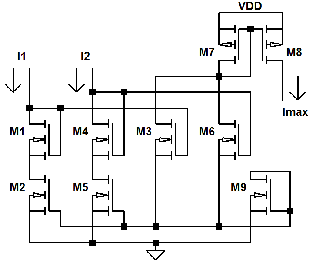
where K, vGS and VT are the device transconductance parameter, the gate-to-source voltage and the threshold voltage, respectively. Suppose that I1 is the largest input current among the two of currents, Imax = max (I1, I2). At steady state, the output current Imax is a replica of the maximum input current, in this case I1. The above discussion confirms the maximum operation. The simplicity of our circuit is responsible for its high speed operation. This circuit can be modified to work as three inputs MAX circuit, as shown in Fig. 4, or as n-input MAX circuit.
Fig. 3. Two input MAX circuit
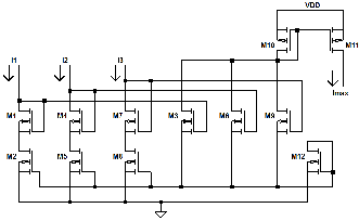
Fig. 4. Three input MAX circuit
To illustrate the above analysis, the performance of the circuit has been simulated using spice. The proposed MIN circuits shown in Fig. 1 & Fig. 2 and MAX circuits shown in Fig. 3 & Fig. 4 can be modified to compute the minimum / maximum current of any number of input currents by increasing the
IJSER © 2013 http://www.ijser.org
International Journal of Scientific & Engineering Research, Volume 4, Issue 4, April-2013 931
ISSN 2229-5518
number of column cells.
The DC transfer characteristic of the proposed two input MIN
circuit with the input current I1 continuously changing from
0µA to 10µA and the other input current I2 changing in steps
of 2µA from 0µA to 10µA is shown in Fig. 5. It confirms that
there is no distortion on the output signal. Fig. 6 and Fig. 7
show the simulated transient response of the proposed two-
input and three-input minimum circuits, respectively. The
supply voltage VDD is equal to 3.3V.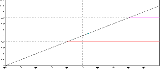
Fig. 5. DC transfer characteristic of two input MIN circuit
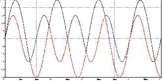
Fig. 6. Transient response of two input MIN circuit
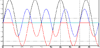
Fig. 7. Transient response of three input MIN circuit
In a similar manner, the DC transfer characteristic analysis and the transient response for the proposed two input MAX circuit is carried out. The DC transfer characteristic response
for a two-input MAX circuit is as shown in Fig. 8. Similarly, the transient response of the two-input MAX circuit and three- input MAX circuit are as shown in Fig. 9 & Fig. 10, respectively. The supply voltage VDD is equal to 3.3V.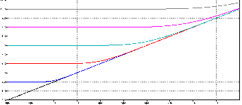
Fig. 8. DC transfer characteristic of two input MAX circuit
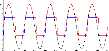
Fig. 9. Transient response of two input MAX circuit
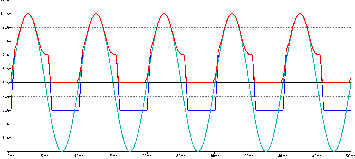
Fig. 10. Transient response of three input MAX circuit
We have presented a very simple current-mode multiple-input minimum and maximum circuit for fuzzy inference system. The multiple input minimum circuits are one-stage circuit with high accuracy and have a large dynamic range. The number of transistors needed for implementing an n-input MIN circuit is only n(n+3) and n-input MAX is only 3(n+1) which is less than the number of transistors used in previous designs. These structures are simple and modular, so it can be easily expanded to meet the requirement of multi-input
IJSER © 2013 http://www.ijser.org
International Journal of Scientific & Engineering Research, Volume 4, Issue 4, April-2013 932
ISSN 2229-5518
signals MIN and MAX circuits. From the simulation results, it is evident that the proposed circuit has the correct function and reasonable degree of precision.
[1] L. A. Zadeh, “Fuzzy Sets,” Information and control, vol. 8, pp.353-383, 1965.
[2] T. J. Ross, “Fuzzy logic with engineering applications,” by John Wiley & Sons
Inc. 2005.
[3] O. Ishizuka, K. Tanno, Z. Tang & H. Matsumoto, “Design of a Fuzzy Controller with Normalization Circuits,” Second IEEE Int. Conf. on Fuzzy Systems, pp.1303-1308, San Diego, CA, USA, March 1992
[4] T. Yamakawa, “A Fuzzy Inference Engine in Nonlinear Analog Mode and its
Application to a Fuzzy Logic Control,” IEEE Trans. on Neural Networks, vol.
4, no. 3, pp. 496-522, May 1993.
[5] R. Amirkhanzadeh, A. Khoei and Kh. Hadidi, “A mixed-signal currentmode fuzzy logic controller,” AEU - International Journal of Electronics and Communications, Volume 59, Issue 3, 9 June 2005, Pages 177-184
[6] S. Aminifar, A. Khoei, Kh. Hadidi and Gh. Yosefi, “A digital CMOS fuzzy logic controller chip using new fuzzifier and max circuit,” AEU - International Journal of Electronics and Communications, Volume 60, Issue 8, 1 September
2006, Pages 557-566.
[7] T. Serrano-Gotarredona and B. Linares-Barranco, “Experimental results on the current-mode WTA-MAX circuit with multichip capability,” in 1997 IEEE Int. Symp. Circuits and Systems (ISCAS’97), Hong Kong, 1997, vol. 1, pp. 561–
564.
[8] R.G. Carvajal, J. Ramirez-Angulo and J. Martinez- Heredia, “High-speed high-precision min/max circuits in CMOS technology,” Electronic Lett., vol.
36, no. 8, pp. 697-699, Apr. 2000.
[9] Batruone J.L. Huertas, A. Barriga and S. Sanchez- Solano, “Current-mode multiple-input Max circuit,” Electronic Lett., vol. 30, no. 9, pp. 678-680, May
1994.
[10] C.Y. Hung, B. D. Liu, “Current-mode multiple input maximum circuit for fuzzy logic controllers,” Electronic Lett., vol. 30, no. 23, pp. 1924-1925, Nov.
1994.
[11] B. Mesgarzadeh, “A CMOS Implementation of Current-Mode Min-Max Circuits and A Sample Fuzzy Application,” Fuzzy Systems, 2004. Proceedings. 2004 IEEE International Conference on Volume 2, 25-29 July
2004 Page(s):941 - 946 vol.2.
[12] M. Soleimani, A. Khoei, Kh. Hadidi, S. KazemiNia, “Design of High- Speed High-Precision Voltage-Mode Max-Min Circuits with Low Area and Low Power Consumption,” IEEE paper. pp. 351-354, Nov. 2009.
[13] T. Inoue, F. Ueno, T. Montoro, O. Setoguchi, and R. Matsuo, “New highspeed analogue max and min circuits using OTA-based boundeddifference operations,” Electron. Lett., vol. 27, pp. 1034–1035, June 1991.
[14] N. Donckers, C. Dualibe, M. Verleysen,“A Current-Mode CMOS Loser-Take- All with Minimum Function for Neural Computations,” Circuits and Systems, 2000. Proceedings. ISCAS 2000 Geneva. The 2000 IEEE International Symposium on Volume 1, Issue , 2000 Page(s):415 - 418 vol.1
[15] H. Watanabe, D. Chen, and S. Konuri, “Evaluation of Min/Max Instructions
for Fuzzy Information Processing,” IEEE Trans. on Fuzzy Systems, vol. 4, pp.
369-374, Aug. 1996.
[16] S. KazemiNia, A. Khoei, Kh. Hadidi,“High Speed High Precision Voltage- Mode MAX and MIN Circuits,” Journal of circuits, systems and computer (JCSC), Vol. 16, No. 2, PP. 233-244, April 2007.
[17] Sasaki, M., Ishikawa N., Ueno, F., Inoue, T, “Current Mode Analog Fuzzy Hardware with Voltage Input Interface and Normalization Locked Loop,” IEICE Trans. Fundamentals, Vol. E75-A (6), June 1992, pp. 650-654.
IJSER © 2013 http://www.ijser.org
International Journal of Scientific & Engineering Research, Volume 4, Issue 4, April-2013
ISSN 2229-5518
933
1-BER IS) 2013
http:1/www.ijserorg